

 中文
Before a multilayer stackup reaches the press, the PCB lamination process starts with an engineering review of the construction and fabrication data. The review decides whether the construction can be built as drawn, which limits apply, and what evidence will verify compliance with the agreed requirements. JetH PCB does not release an unclear build.
If you are preparing files for a multilayer PCB prototype or low-volume run, the checks below decide whether your stackup proceeds, comes back with questions, or gets revised before a single sheet of prepreg is cut.
Published by JetH PCB
Where Lamination Fits in the Multilayer Build
In a multilayer PCB manufacturing process, the first lamination in a conventional flow sits after inner-layer imaging and AOI, before through-hole drilling and plating. Sequential constructions can place drilling and plating between lamination stages, which is why the route is reviewed per build. After etching, each inner-layer pattern can still be inspected directly. AOI can identify visible pattern defects, such as unintended copper breaks, bridges and missing features, while the layers are still individual sheets. Once the book is pressed, internal layers cannot be inspected directly from the finished surface. Required destructive checks, test coupons and acceptance limits should therefore be defined before the construction is released.
The pre-press review is the last point where the construction exists entirely as data that can still be changed cheaply.
The Engineering Release Gate: What Is Checked Before Lamination
JetH's engineering review works through five categories of input before a build is released:
- Files. Gerber or ODB++ data, NC drill files, the fabrication drawing, and the part number with its revision. The first check is whether these describe the same board; a disagreement between revisions or limits stops the release until one definition is approved.
- Construction. Layer count, board thickness, copper weights, materials and via construction. The question is whether the proposed core and prepreg build can deliver the finished thickness, copper weight and via spans requested.
- DFM. Trace and space widths, drill sizes, annular rings and edge clearance. They are checked against the construction, not a generic rule, because the allowable trace, drill and ring change with copper weight and layer count.
- Impedance. The stack-up, dielectric thicknesses, trace geometry and the tolerance the design targets. The review checks whether the target can be held across the stackup, not just one test layer.
- Approval. CAM changes, conflicts between documents, and any material alternatives proposed before anything is committed. Changes are raised with the customer before release; nothing is substituted silently.
Typical release blockers include a revision or dimension conflict between the Gerber set and the drawing; a finished thickness the chosen core and prepreg cannot deliver; an annular-ring margin that does not survive the specified drill and registration requirements; an impedance target the proposed stackup cannot hold; and a CAM change or material substitution that changes the approved definition.
Production timing is confirmed only after the files are complete, technical questions are closed and the order is released.
Stackup Review: What Makes a Construction Manufacturable
A stackup that simulates correctly in your EDA tool is not automatically a buildable board. Stackup review at JetH covers the core and prepreg combination, copper weights, reference layers, dielectric thickness, finished thickness, symmetry of the construction, and the via construction, all checked against each other before fabrication.
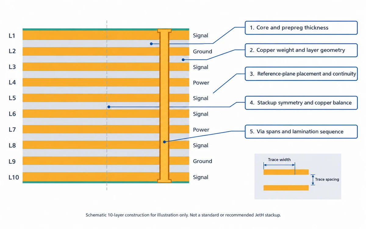
The stated limits show where the boundaries sit. Minimum core thickness is 50 μm and minimum prepreg thickness is 40 μm for production builds (40 μm and 30 μm, respectively, for samples). They are construction-input limits, not guaranteed finished dielectric thicknesses; the target pressed dielectric is defined in the approved stackup. For non-HDI production, the stated maximum finished thickness is 7.0 mm; a specific thickness is still evaluated against the complete construction and order conditions. Layer count is rated separately: up to 28 layers for non-HDI production and up to 40 for qualifying samples. Published low-volume limits use delivery area instead: up to 40 layers below 5 m² and up to 20 at or above 5 m². These describe different order conditions and are not interchangeable guarantees.
None of those limits should be read as combinable. As JetH's capability pages state, maximum limits may not be combinable: a 40-layer sample board cannot also assume maximum thickness and the tightest dielectrics. Final feasibility is confirmed from the complete construction.
Material suppliers publish their own processing guidance — Rogers' RO4000 fabrication documentation, for example — but those recommendations are material-specific and do not replace the approved stackup.
Electrical feasibility and manufacturability diverge here. A four-layer board with unusually thin dielectrics may meet the impedance target and still fail review because the prepreg cannot guarantee dielectric control at that thickness with the requested copper weight. An asymmetric copper distribution may trigger a review of symmetry and copper balance; the fix may be revised copper distribution, a different layer arrangement or another approved stackup change. Via architecture also shapes the route. Some blind-via, buried-via and HDI constructions may require sequential lamination; through vias do not automatically add cycles. Back drilling and via-in-pad filling or copper capping are separate processes reviewed alongside the stackup. For simpler layer-count and dielectric choices, see the 4-layer PCB stackup guide.
Layer Registration: Risk Factors and Review Actions
Layer registration, the alignment between copper features on different layers after pressing, is treated at JetH as a control point separate from fine circuitry, plated holes and impedance. That separation matters because registration cannot be summarized as one machine's accuracy rating.
Registration risk accumulates from the construction itself: layer count, board thickness, copper distribution, the annular-ring budget and whether the build includes blind or buried vias. Two designs can pass through the same press with very different outcomes because the designs, not the press alone, set the margin.
The stated design constraints define part of that margin. Minimum annular rings are 89 μm for inner layers and 75 μm for outer layers in production for mechanically drilled holes (75 μm and 64 μm for samples), and 50 μm for laser-drilled holes in production (40 μm for samples). These are minimum annular-ring requirements, not layer-to-layer registration tolerances. They define part of the geometry that must survive fabrication; the acceptable registration margin is evaluated separately against the drilling data, layer alignment requirements and specified acceptance limits.
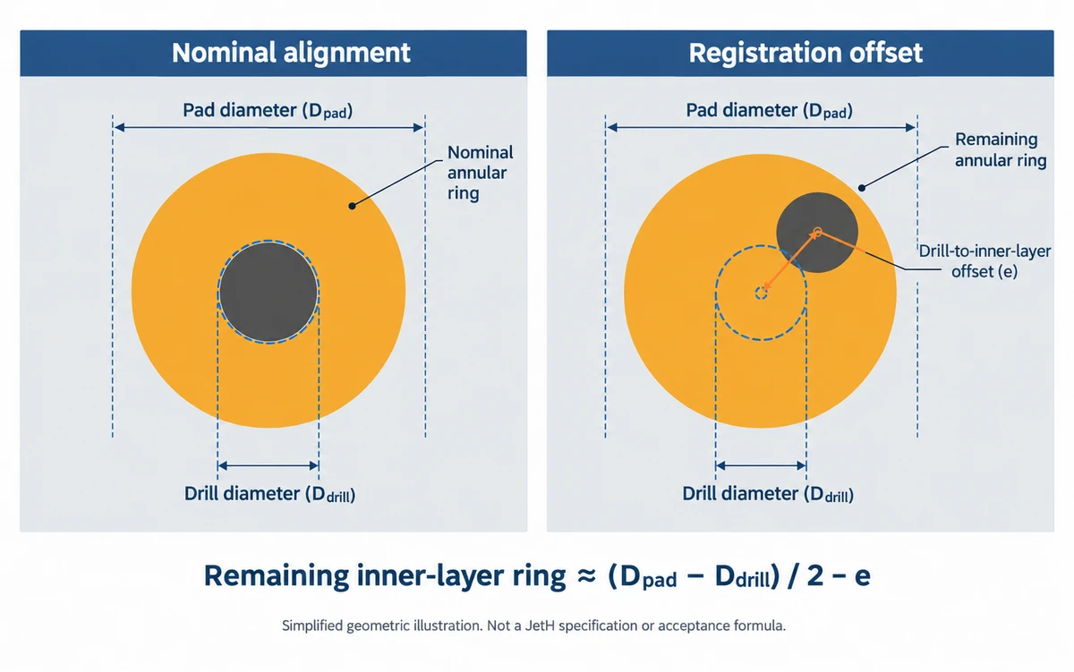
There is no single registration tolerance that applies to every multilayer construction. The applicable requirement and verification method are evaluated against the specific stackup, drilling data and agreed acceptance criteria. Inner-layer AOI verifies copper patterns against the approved design data before lamination. Post-lamination registration is assessed through the registration controls and inspection steps defined for the build. Microsection can examine internal layer relationships and hole copper at agreed locations, but it provides local evidence rather than full-board, non-destructive coverage.
Sequential Lamination and Hybrid Constructions
Some HDI constructions with blind or buried vias cannot be pressed in a single cycle and require sequential lamination, where sub-composites are built up in stages before the final press. The applicable sequence depends on the via architecture and the complete stackup.
JetH publishes different lamination-cycle limits for mechanical blind and buried vias by delivery area. For orders below 5 m², the published limit is stated as fewer than three lamination cycles; for orders of 5 m² or more, it is stated as fewer than two. Constructions outside these limits require engineering review. Hybrid builds appear in the company's representative constructions: ceramic-and-FR4 and Rogers/PTFE high-frequency hybrid stackups. Mixed materials bring different thermal expansion behavior into the same book, which is exactly what the stackup review is meant to surface.
Those published limits are a starting boundary, not a guarantee that every construction inside them is combinable. The applicable sequence is determined by the via architecture and confirmed from the complete construction during engineering review.
What Inspection Methods Can and Cannot Verify
Because critical internal features cannot be inspected directly from the finished surface, the inspection plan must account for how each feature will be verified. Each method provides evidence about specific characteristics, and no single method covers every manufacturing risk:
| Method | What it can verify | What it does not cover |
|---|---|---|
| Inner-layer and outer-layer AOI | Circuit-pattern defects and conformity to approved design data on inspected layers | Internal interfaces and final post-lamination registration |
| Microsection | Internal structure and hole copper at agreed locations | The whole batch; it is a sectioned sample, not a non-destructive full inspection |
| Flying probe or fixture electrical test | Opens, shorts and isolation against the netlist | Lamination defects that do not yet affect continuity |
| Impedance coupon with TDR and report | Whether the agreed impedance targets are met | Impedance of every net on the board |
| Final visual inspection | Visible defects on the finished board | Internal structure |
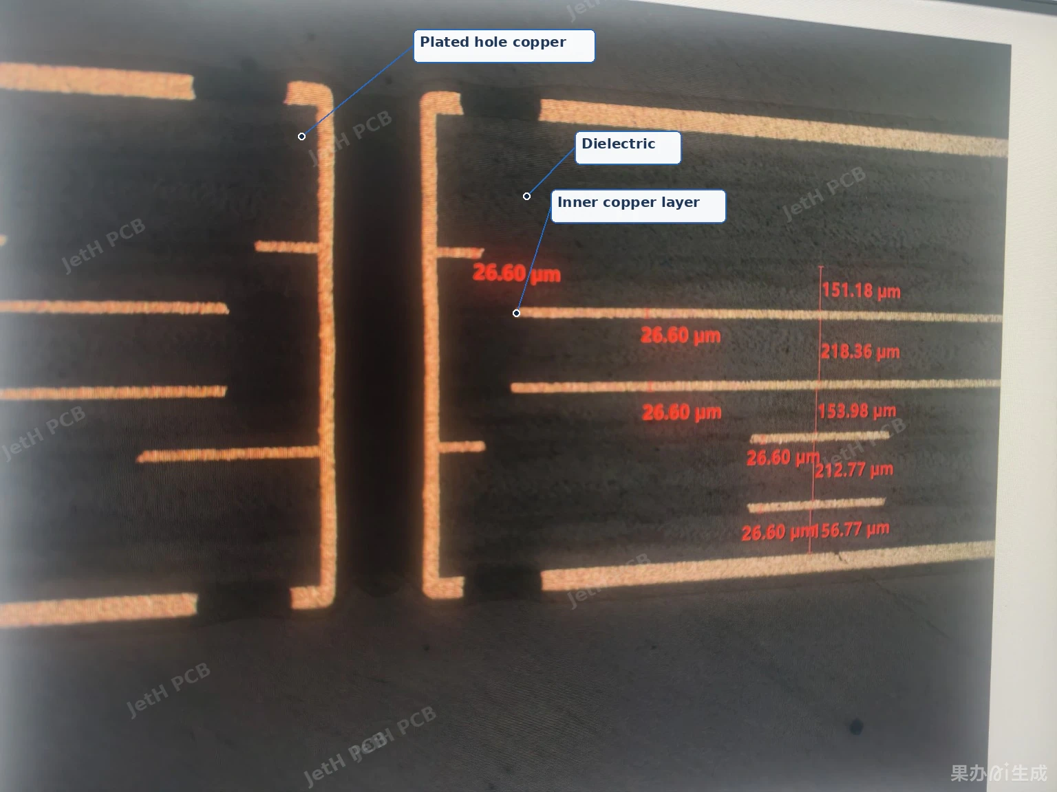
Acceptance classes and test methods are defined in IPC-6012, the qualification and performance specification for rigid printed boards; the applicable class is agreed for the order.
Impedance tolerance is settled by the construction and the acceptance requirements agreed for the order, not by a single figure. Where impedance is specified, it is verified with coupons and TDR, and the report requirement is agreed at quotation. Other agreed evidence can include copper thickness measurement, ionic cleanliness, peel strength and a certificate of conformance. Inspection frequency and first-article requirements are defined in the inspection plan agreed before production.
The practical takeaway for a designer: specify the evidence you need at quotation. If a microsection is required, agree on its location and acceptance limits before production. Adding a representative inspection location after pressing may not be practical.
PCB Lamination DFM Checklist for an RFQ
The review starts from what you send. For a multilayer RFQ, JetH asks for:
- Gerber or ODB++ files
- NC drill files
- The fabrication drawing
- Part number and revision
- Stackup drawing and construction details, including layer count, material grades, copper weights and finished board thickness
- Board dimensions
- Quantity and delivery requirement
- Material and surface finish
- Testing and report requirements
If the design uses controlled impedance, include the target impedance, the controlled signal layers, the reference layers, the design tolerance and the test report requirement.
One timing note that is easy to miss: lead time starts when the files are complete, technical questions are closed and the order is released. A stackup sent without the fabrication drawing does not start the clock; it starts a conversation.
Frequently Asked Questions
What files does a manufacturer need to review a multilayer stackup?
Gerber or ODB++ data, NC drill files, the fabrication drawing, and the part number with revision. For constructions outside the standard range, send the stackup and fabrication drawing together; final feasibility is confirmed from the complete construction.
Is there a universal layer-registration tolerance?
No single figure applies to every multilayer construction. Registration depends on layer count, board thickness, copper distribution, the annular-ring requirement and the drilling data. JetH reviews it against the specific construction and does not publish one universal tolerance.
Can a manufacturer change my stackup?
CAM changes and material alternatives are part of the approval step, and any proposed change is raised with you before production. You approve one build definition before the order is released; nothing is changed silently after that.
Which tests should I specify before quotation?
Decide up front which evidence the order requires: impedance coupons with TDR and report, microsection, electrical test method (flying probe or fixture), and any additional measurements such as copper thickness or ionic cleanliness. Inspection frequency and first-article requirements are defined in the inspection plan agreed before production.
For more background on stackup, via and inspection topics, browse the JetH PCB Guide.