

Multilayer PCB

Your Direct PCB & PCBA Manufacturing Partner

Multilayer PCB
Home PCB Catalogue Multilayer PCB
Custom Multilayer PCB Fabrication

Multilayer PCB Manufacturer

Reliable multilayer PCB manufacturing for projects requiring controlled impedance,custom stackups, precise layer registration, complex via structures and consistent electrical performance.
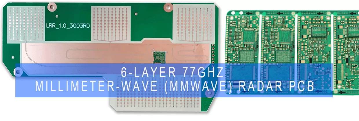
6-Layer 77GHz Millimeter-Wave (mmWave) Radar PCB
Manufacturing Capabilities

Multilayer PCB Manufacturing Capabilities

Layer count, stackup, dielectric construction, via structure and impedance requirements must be considered together for reliable multilayer PCB fabrication.

Send Your PCB Files →
Layer Count
Up to 40 Layers
Min Trace / Space
Down to 3/3 mil
Min Drill
4 mil
Impedance Control
Available
Board Thickness Custom Copper Weight Up to 20 oz External / 10 oz Internal
Blind / Buried Via Available Aspect Ratio Up to 20:1
Materials FR-4 · High-Tg · PTFE · Hybrid Testing Electrical Test
+ View additional multilayer PCB capabilities
Surface finishes: ENIG, HASL, OSP, immersion silver, immersion tin, hard gold and flash gold. For specifications outside the standard range, send your stackup and fabrication drawing for engineering review.
Key Multilayer PCB Capability

Controlled Impedance Multilayer PCB

Controlled impedance depends on the complete multilayer construction. Dielectric thickness, copper thickness, trace geometry, spacing and reference planes must be controlled together during fabrication.
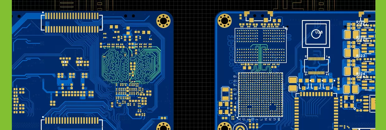
Controlled Impedance Multilayer PCB Stackup
Stackup · Dielectric · Trace Geometry · Reference Plane
Single-Ended & Differential
Custom impedance targets according to your PCB requirements.
Stackup Review
Core, prepreg, copper and reference layers checked before fabrication.
Impedance Verification
Impedance verification according to specified requirements.
Manufacturing Control Path
Target Impedance → Stackup → Dielectric → Trace Geometry → Fabrication → Verification
+ What information should I provide for controlled impedance fabrication?
• Target impedance values
• Required tolerance
• Controlled signal layers
• Reference layers
• Trace width / spacing
• Proposed stackup
• Copper weight
• Material requirements
Construction & Manufacturability

Multilayer Stackup, Layer Count & Via Structure

Stackup, layer count and via construction are reviewed as one manufacturing system rather than isolated specifications.
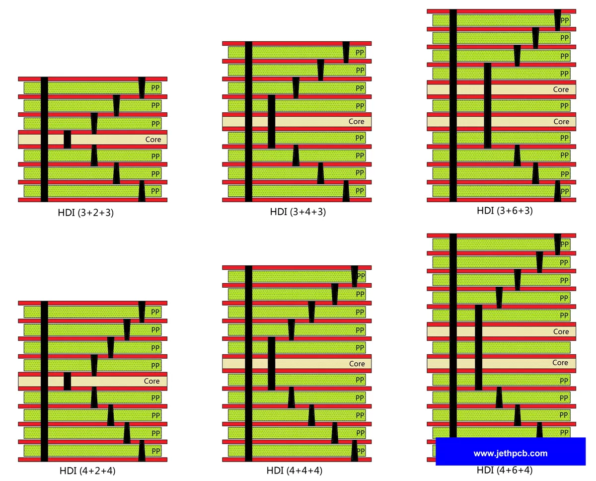
Comparison of six HDI multilayer PCB stackups showing layer counts, cores, prepreg and through, blind and buried via structures reviewed for manufacturability.
01

Custom Multilayer PCB Stackup

Signal, ground and power layers are reviewed together with core/prepreg thickness, copper construction and controlled impedance requirements.

+ View stackup considerations
Core and prepreg · dielectric thickness · finished thickness · copper thickness · symmetry · via construction.
02

4-Layer to High-Layer-Count PCB

Support for 4, 6, 8, 10, 12, 14, 16 and high-layer-count multilayer PCB fabrication up to 40 layers.

+ View high-layer-count considerations
Board thickness · drill diameter · registration · aspect ratio · copper distribution · impedance.
03

Blind & Buried Via Multilayer PCB

Through vias, blind vias, buried vias, via-in-pad and back drilling can be reviewed according to the actual multilayer construction.

+ View via manufacturability factors
Hole diameter · layer span · annular ring · aspect ratio · copper thickness · lamination structure.
04

Multilayer PCB DFM & Engineering Review

Check stackup feasibility, drill-to-thickness ratio, via construction, layer registration, copper distribution and impedance requirements before production.

Submit for DFM Review →
Multilayer PCB Quality Control

Control What Cannot Be Seen After Lamination

Critical multilayer PCB features are internal, so process control begins before final lamination.

01 Inner-Layer AOI
02 Layer Registration
03 Lamination Control
04 Hole Metallization
05 Electrical Testing
Multilayer PCB FAQ
Why do high-speed circuits often use multilayer PCBs?
Multilayer PCBs allow signal layers to sit next to continuous reference planes while providing dedicated ground and power distribution, helping improve return-path control and reduce EMI and crosstalk. View High-Speed PCB →
How do you handle multiple voltages in a multilayer PCB?
Multiple voltage rails may use dedicated power planes, divided power regions or routed power structures depending on current requirements, available layers and reference-plane continuity.
How is controlled impedance verified on a multilayer PCB?
The finished construction is controlled through dielectric thickness, copper thickness, trace geometry and reference-plane position. Verification requirements are reviewed according to the PCB specification.
What should be considered before manufacturing a multilayer PCB?
Key considerations include stackup, board thickness, core and prepreg construction, copper thickness, trace/space, drill dimensions, aspect ratio, via structure, layer registration, controlled impedance and manufacturing tolerances.

Get a Multilayer PCB Quote

Send your Gerber or ODB++, stackup, layer count, material, copper weight, via requirements and controlled impedance specifications for engineering review.

Get Expert Support

Our team will get back to you within 24 hours


DFM & Design Review DFM & Design Review

Technical ConsultationTechnical Consultation

Fast ResponseFast Response

How can we help you?
Name*
Email*
Company Name*
Address
Job Title
Phone Number
Message
Upload Gerber/PCB File:
Send Message
Name*
Email*
Company Name*
Address
Job Title
Phone Number