
Home PCB Technology& Solution PCB Manufacturing Facilities
PCB Manufacturing Equipment

PCB Manufacturing Equipment & Production Facilities

Our PCB manufacturing facility combines digital imaging, precision drilling, multilayer lamination, copper metallization, surface processing and automated inspection equipment to support prototype and low-volume printed circuit board production. Each production stage is controlled by trained operators and verified through in-process inspection, electrical testing and final quality checks.

7
Core Equipment Categories
40 Layers
Maximum Multilayer Capability
3/3 μm
Minimum Line/Space
100%
Electrical Testing as Required
Explore JetHPCB

Need More Than an Equipment List?

Continue with the information most relevant to your supplier evaluation: who we are, where we have industry experience, or the manufacturing parameters we support for prototype and low-volume PCB builds.

Inside Our Facility

PCB Production Equipment Gallery

PCB Manufacturing Facilities
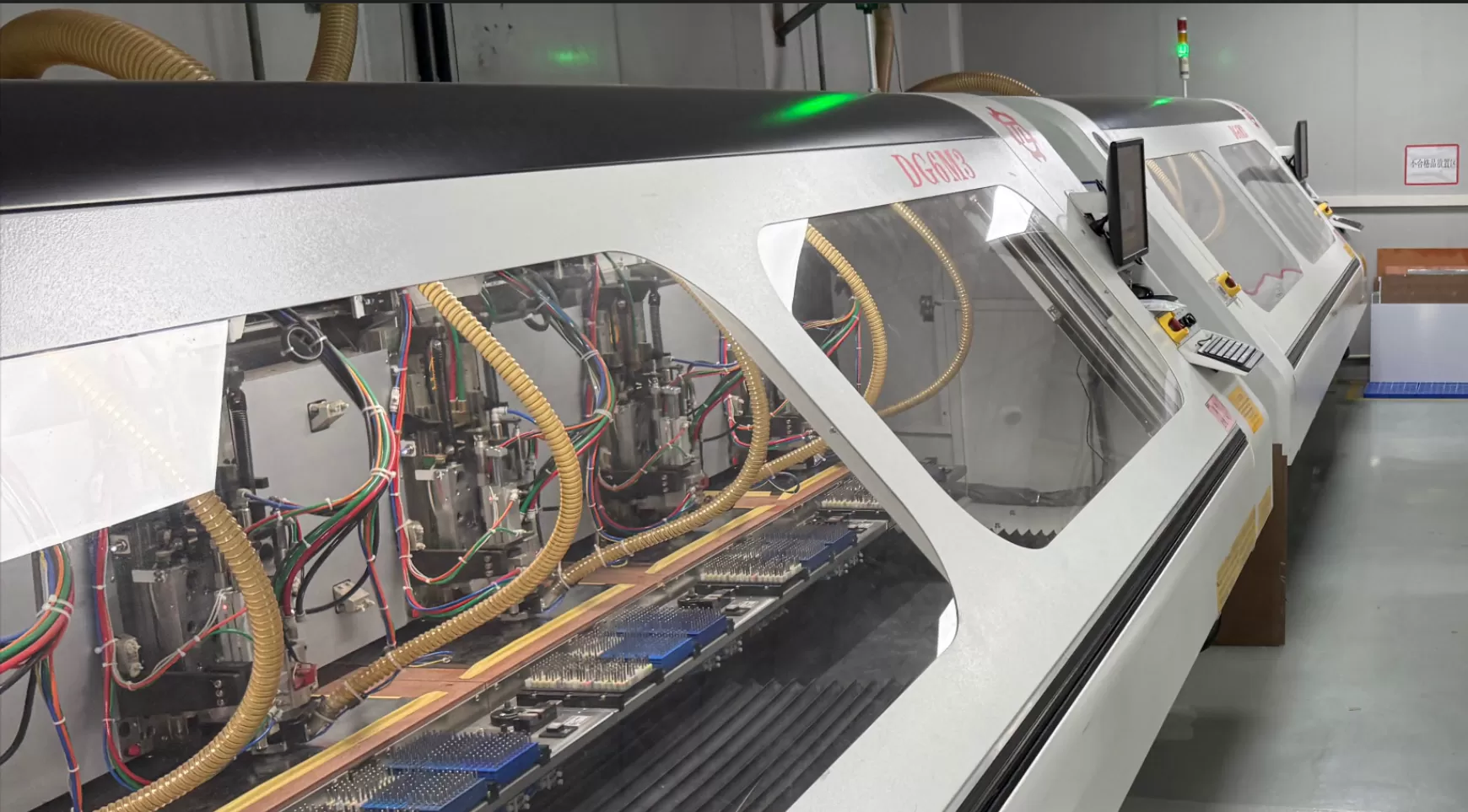
CNC drilling and routing machine
PCB Manufacturing Facilities
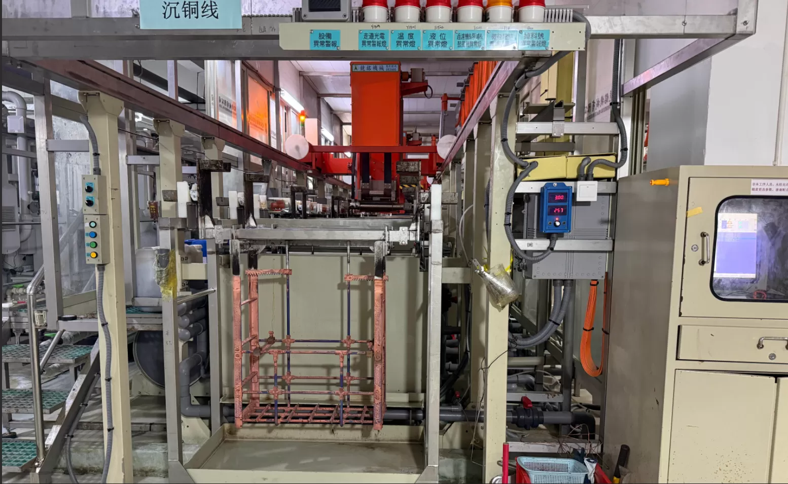
Copper plating and hole metallization line
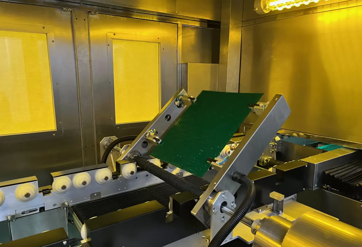
Automatic solder mask printing and curing equipment
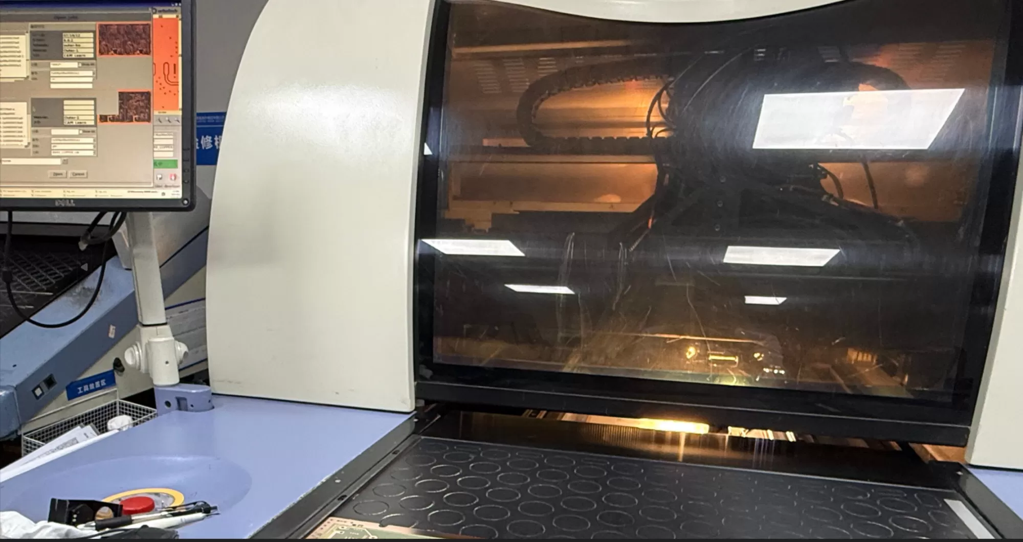
AOI and electrical testing equipment
Equipment-to-Capability

How Our Equipment Supports PCB Manufacturing

Select a production stage to see how the equipment contributes to PCB precision, repeatability, turnaround and quality control.
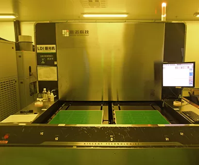
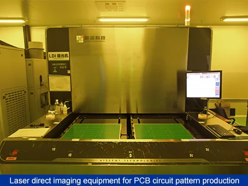
Laser direct imaging equipment for PCB production
Equipment Role 01

Laser Direct Imaging

Digital imaging transfers circuit patterns directly to the production panel without conventional film. It supports tighter registration, consistent image reproduction and fine-line PCB manufacturing.

Process
Circuit Imaging
Capability Value
Fine Lines & Registration
What Equipment Should Prove

Evaluate Capability, Not Machine Names Alone

A useful equipment review should connect each machine with a qualified manufacturing range, inspection method and production result.

01

In-House Processes

Confirm which critical processes are performed internally and which are managed by approved external partners.

02

Qualified Tolerances

Compare the qualified production range with your line width, hole size, layer count, copper and registration requirements. Review prototype & low-volume technical capability →

03

Capacity & Redundancy

Review equipment quantity, available capacity and backup arrangements for critical production stages.

04

Inspection Coverage

Check whether AOI, electrical testing, impedance measurement and laboratory inspection match the PCB risk level.

Buyer Questions

PCB Manufacturing Equipment FAQ

How can buyers verify that critical PCB processes are performed in-house?
Review factory photographs, equipment models, production-flow records and process-control documentation. Buyers should identify which stages—such as imaging, drilling, lamination, plating, surface finishing and electrical testing—are completed internally. When a process is outsourced, the PCB supplier should explain how the subcontractor is qualified, monitored and traced.
Does advanced equipment automatically guarantee tighter PCB tolerances?
No. Machine capability must be supported by a qualified manufacturing process, calibrated measurement systems, controlled materials and experienced operators. Buyers should compare the factory’s released production limits—not only the machine brochure—with the required line width, spacing, finished hole size, registration tolerance, copper thickness and impedance tolerance.
What equipment is most important for multilayer and HDI PCB production?
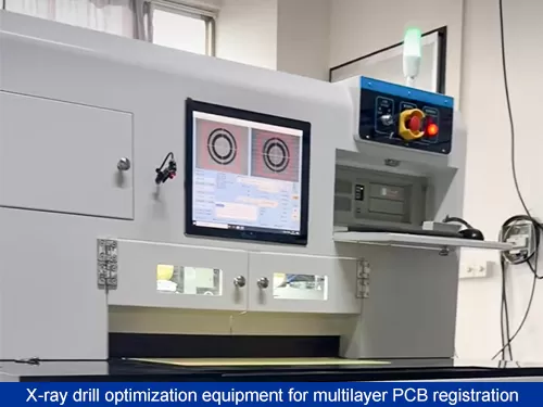
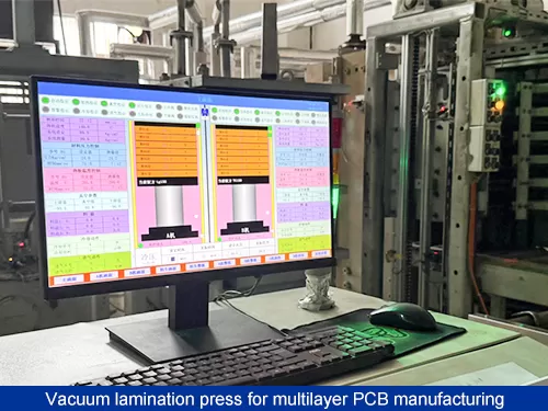
Important equipment can include laser direct imaging, X-ray registration, precision CNC or laser drilling, vacuum lamination presses, plasma desmear, controlled metallization and plating lines, AOI and electrical testing systems. The correct combination depends on the layer count, microvia structure, material system, aspect ratio and registration requirements of the PCB.
How should buyers evaluate equipment capacity and production reliability?
Buyers should review the number of critical machines, typical utilization, supported panel sizes, production shifts, preventive-maintenance plans and backup arrangements. A factory with one advanced machine may still have a delivery risk if there is no redundancy or qualified alternative when maintenance is required.
Which PCB inspection and testing capabilities should be available?
Inspection coverage should reflect the PCB’s technical and reliability risks. Common controls include inner- and outer-layer AOI, flying-probe or fixture electrical testing, impedance measurement, copper and surface-finish thickness measurement, microsection analysis and final visual inspection. High-reliability projects may also require additional thermal, cleanliness or material verification.

Discuss Your PCB Manufacturing Requirements

Send us your Gerber files, stack-up, material requirements and target tolerances. Our engineering team will review the production process and confirm the applicable manufacturing and inspection capabilities.

Get Expert Support

Our team will get back to you within 24 hours


DFM & Design Review DFM & Design Review

Technical ConsultationTechnical Consultation

Fast ResponseFast Response

How can we help you?
Name*
Email*
Company Name*
Address
Job Title
Phone Number
Message
Upload Gerber/PCB File:
Send Message
Name*
Email*
Company Name*
Address
Job Title
Phone Number