Open Nav


Ask for Tech Support
JetH PCB manufactures bare PCBs for automotive electronics, EV and energy systems, RF communication, industrial controls and other technically demanding products.
We do not reduce manufacturability to one headline number. Materials, copper construction, hole structures, impedance, mechanical limits and inspection requirements are evaluated as one production system.
Request a PCB Review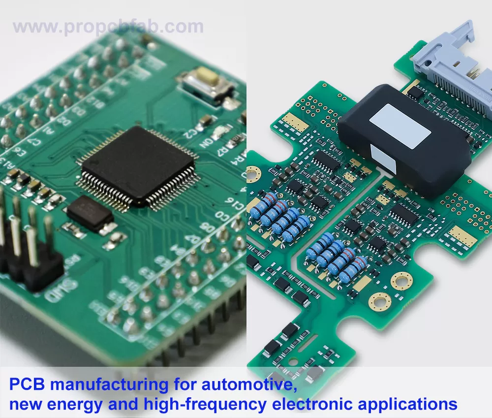
A capable PCB supplier must understand what the board is expected to survive, control and transmit.
JetH PCB connects fabrication decisions with current load, voltage, signal behavior, thermal exposure, mechanical stress and product-life expectations.
Every project receives its own material, stack-up, registration, surface-finish and verification strategy. We do not force unrelated applications into the same manufacturing recipe.
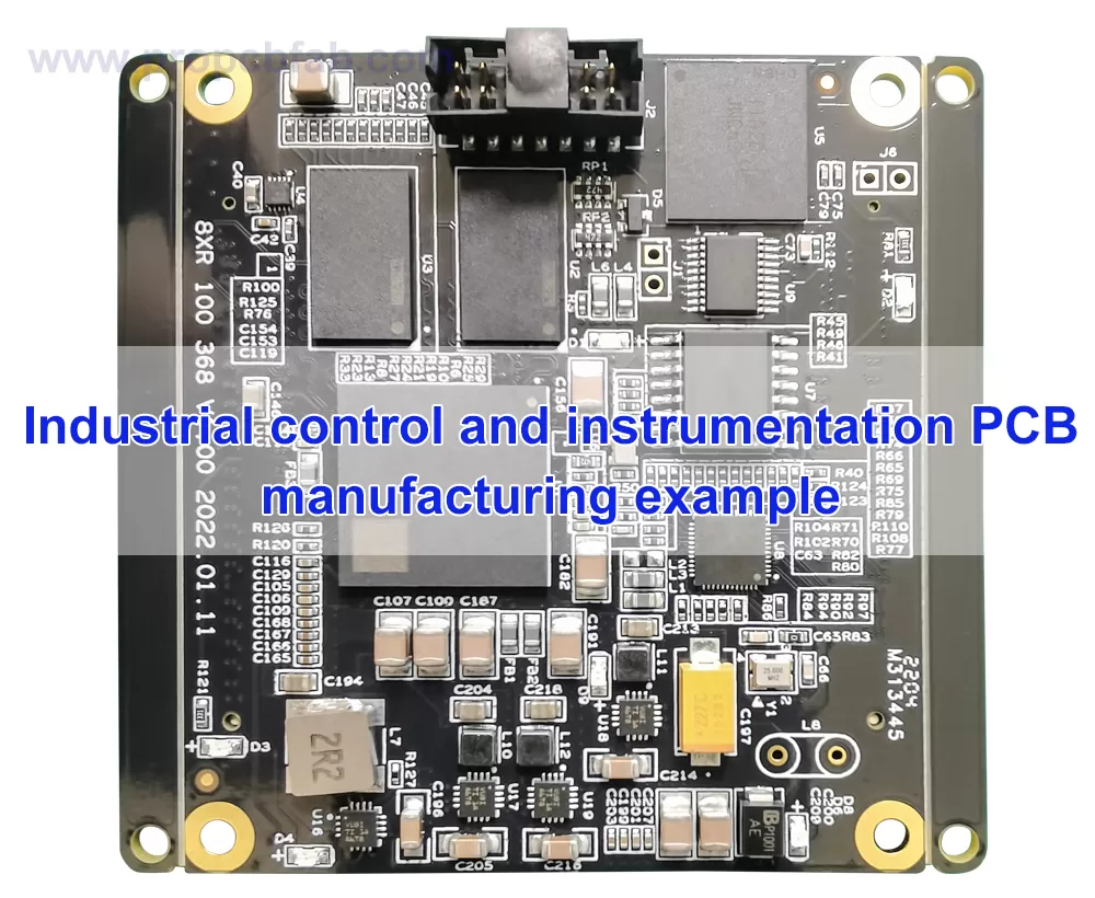
JetH PCB challenges weak assumptions before they become production defects. The application determines which risks deserve the most attention.
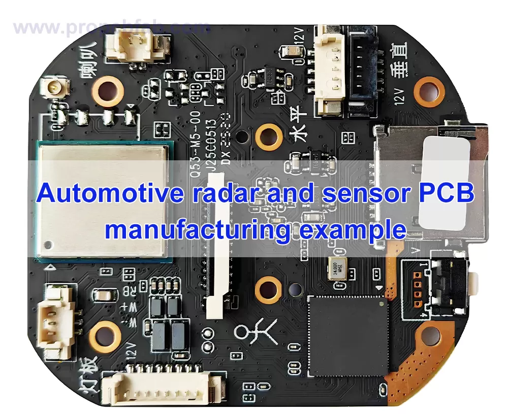
Temperature cycling, vibration, electrical transients and long service life expose manufacturing weaknesses quickly. We align the fabrication plan with the needs of ADAS radar PCBs, vehicle sensors, control units, lighting modules and communication systems.
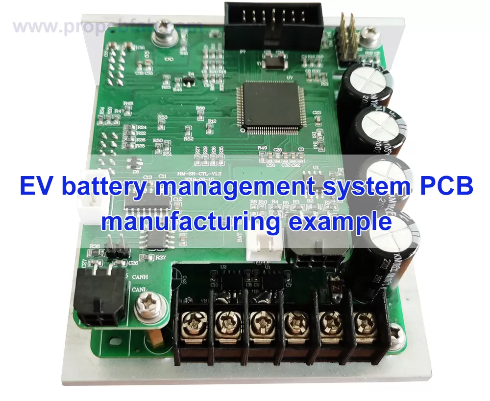
High current, elevated voltage and concentrated heat demand deliberate conductor geometry and isolation planning. Our engineers examine copper distribution, thermal paths, creepage, clearance and finished thickness for EV BMS PCBs, energy storage, on-board chargers, DC-DC converters and charging equipment.
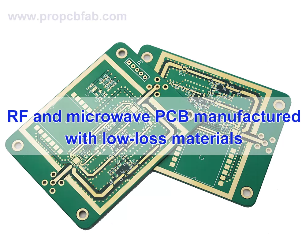
At high frequencies, laminate selection and manufactured geometry directly affect electrical behavior. JetH Pro PCB Fab controls the relationship between dielectric properties, copper profile, trace dimensions and registration for radar, microwave, antenna and high-speed communication boards.
JetH PCB publishes capability by delivery area because PCB prototype and volume conditions are not identical. Extreme values remain construction-dependent and must be approved together through DFM review.
| Capability | Delivery Area <5 m² | Delivery Area ≥5 m² |
|---|---|---|
| Layer Count | 1–40 layers | 1–20 layers |
| Board Thickness | 0.20–7.00 mm without solder mask 0.40–7.00 mm with solder mask | 0.30–5.00 mm without solder mask 0.40–5.00 mm with solder mask |
| Maximum Finished Copper | Internal: 10 oz External: 20 oz | Internal: 5 oz External: 10 oz |
| Minimum Trace / Space | Internal: 3/3 mil at 1/2 oz External: 3/3 mil at 1/3 oz | Internal: 3/3 mil at 1/2 oz External: 3.5/4 mil at 1/3 oz |
| Finished Mechanical Hole | 4–244 mil 0.10–6.20 mm | 5–244 mil 0.13–6.20 mm |
| Laser Microvia | 4–6 mil laser drill 4–5 mil for filled laser vias | 4–6 mil laser drill 4–5 mil for filled laser vias |
| Controlled Impedance | ±10% | ±10% |
| Blind / Buried Vias | Mechanical blind and buried vias with fewer than 3 lamination cycles | Mechanical blind and buried vias with fewer than 2 lamination cycles |
| HDI Construction | 1+n+1, 1+1+n+1+1, 2+n+2 and 3+n+3 | 1+n+1, 1+1+n+1+1, 2+n+2 and 3+n+3 |
| Surface Finishes | ENIG, ENEPIG, OSP, lead-free HASL, leaded HASL, hard gold, soft gold, flash gold, immersion silver and immersion tin | |
| Material Families | FR-4, high-Tg FR-4, Rogers, Taconic, Arlon, Nelco, PTFE and hybrid constructions | |
Gerber files describe geometry. They do not explain why the board needs a particular material, copper structure, isolation distance or inspection standard.
JetH Pro PCB Fab uses application information to identify manufacturing risks before tooling and production release.
Temperature range, humidity, vibration, installation location and expected service life.
Working voltage, current, frequency, data rate, target impedance and isolation requirements.
Layer stack-up, material grades, base and finished copper, via architecture and surface finish.
Electrical testing, impedance reports, microsection analysis, material documentation and first-article approval.
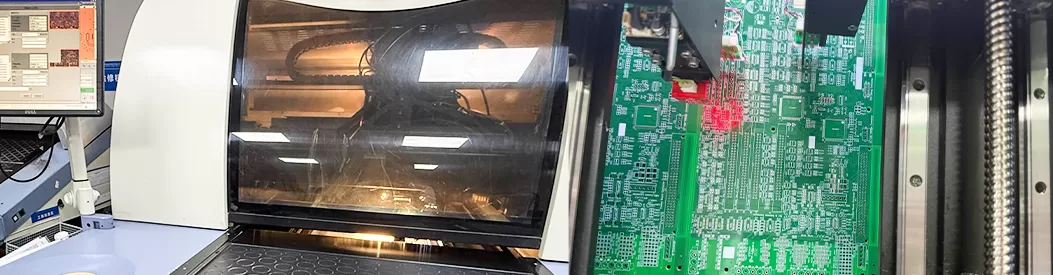
Send the Gerber data, stack-up, material requirements and operating conditions. JetH Pro PCB Fab will define the practical manufacturing and inspection path before production.
Our team will get back to you within 24 hours
 DFM & Design Review
 Technical Consultation
 Fast Response
 中文