Open Nav
Ask for Tech Support
HDI PCB MANUFACTURING
Founded in 2003, JetH PCB has continued to develop its HDI PCB manufacturing processes as electronics technology advances. Our experience spans AI servers, 5G communications, and industrial automation.
Thanks for the years of manufacturing HDI boards for different projects, we work with different HDI build-up structures and BGA escape routing requirements with a good understanding of how to match the board structure to the BGA routing needs.
For HDI PCBs, our focus is on layer registration during lamination, laser-drilling tolerances, complete resin filling, and a flat surface finish.
Request an HDI PCB Review →Useful files: fabrication data, stack-up, drawing, target quantity and critical BGA or via requirements.
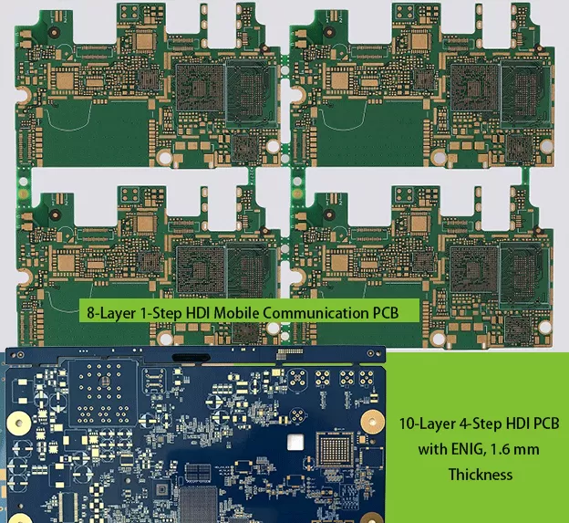
For the fine traces and Laser-drilled blind microvias requirements, we typically can go down to 65 μm in production and 50 μm for prototypes. With ½ oz inner-layer copper, minimum trace/space reaches 35/40 μm; for 20 μm outer-layer copper, it is 45/50 μm.
The production range includes HDI boards up to 18 layers, 4+N+4 structures, and any-layer interconnects. Prototype capabilities extend to 32 layers and 5+N+5 structures, with any-layer options also available.
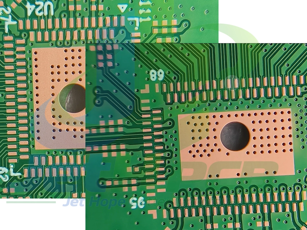
PCB microscope view: copper thermal pad with closely spaced thermal vias.
We support resin-filled, copper-capped via-in-pad (VIPPO) and operate a fully automatic vacuum via-filling line.
Before production, we review the via-in-pad dimensions, resin-fill and copper-cap requirements, annular rings, and registration allowances. We confirm these details with you before production.
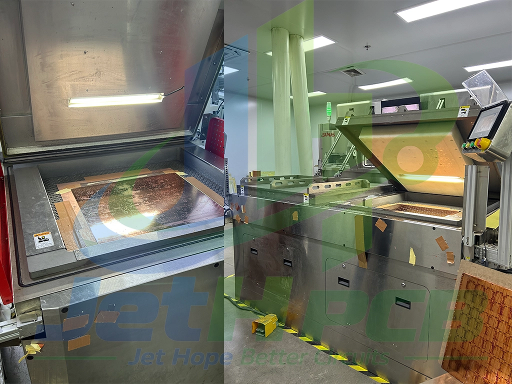
Fully automatic vacuum via-filling line.
Surface profile measurements show any dips or raised areas on the VIPPO copper caps, along with height differences relative to the surrounding BGA pads. We use these measurements to check surface planarity after via filling and copper capping.
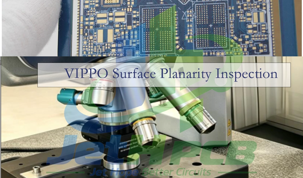
Surface profile measurement for VIPPO planarity inspection.
| HDI Parameter | Volume Production | Prototype |
|---|---|---|
| Maximum HDI layer count | 18 layers | 32 layers |
| HDI build-up structure | Up to 4+N+4 | Up to 5+N+5 |
| Any-layer interconnects | Available | Available |
| Maximum HDI board thickness | 3.0 mm | 3.6 mm |
| Minimum laser-drilled blind via diameter | 65 μm | 50 μm |
| Maximum blind via aspect ratio | 1:1 | 1.2:1 |
| Minimum laser via annular ring | 50 μm | 40 μm |
| Maximum laser drilling depth for L1–L3 vias | 250 μm | 300 μm |
| Minimum inner-layer trace/space — ½ oz copper | 35/40 μm | 25/30 μm |
| Minimum inner-layer trace/space — 1 oz copper | 40/50 μm | 30/35 μm |
| Minimum outer-layer trace/space — 20 μm copper | 45/50 μm | 40/40 μm |
| VIPPO resin-filled blind via diameter | 0.20–0.30 mm | 0.15–0.50 mm |
| Maximum aspect ratio for resin-filled blind vias | 0.9:1 | 1.2:1 |
Our engineering team will automatically identify the BGA pitch, pin count, via-in-pad distribution from your Gerber, confirm the required 1+N+1/2+N+2 HDI stackup, verify that your 2.5mil trace/space and 75μm microvia design are fully compatible with our production capacity, and then give you a fixed price without hidden extra charges. We will only contact you if we find any design risks that may affect yield, and provide 2 optimized cost-down options for you to choose.
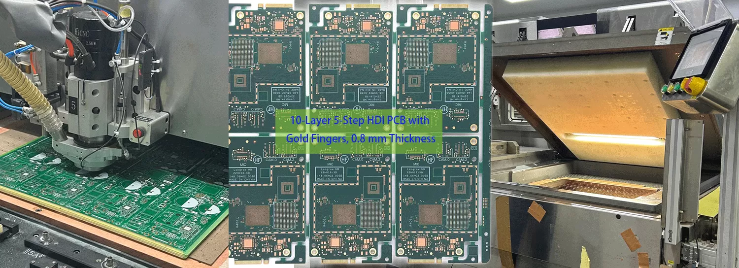
Finished HDI PCB with gold fingers.
Ordering a small initial run? Include the expected repeat quantity as well. That gives us the context to discuss the same HDI construction across both stages.
To see our wider board range, visit PCB manufacturing capabilities. For factory and process information, see PCB manufacturing.
Share Prototype and Repeat-Order Quantities →JetH PCB can deliver a locked, production-ready quotation purely from your Gerber files, no extra design documents required.
Our process is:
The price we quote from Gerber will not change at the production stage, and we guarantee the via-in-pad coplanarity ≤15μm for your BGA region, with 98.5% first-pass yield.
If your team has already approved a structure, include it. If the build-up is still under review, send the required layer connections and BGA routing information so we can discuss the proposed construction.
Our HDI prototype specification is 100% transferable to repeat production, no requalification required.
We implement a full "golden sample" management system for every fine-pitch BGA HDI project:
We guarantee that the repeat production boards will be electrically and mechanically identical to your validated prototype, with zero design or process drift. If any parameter deviation is found, we will rework the batch for free.
Share your files, proposed stack-up and order quantity. Add a note about any routing or microvia detail your team wants us to check.
Request a Fine-Pitch BGA HDI PCB Quote →Our team will get back to you within 24 hours
 DFM & Design Review
 Technical Consultation
 Fast Response
 中文