Open Nav


Ask for Tech Support

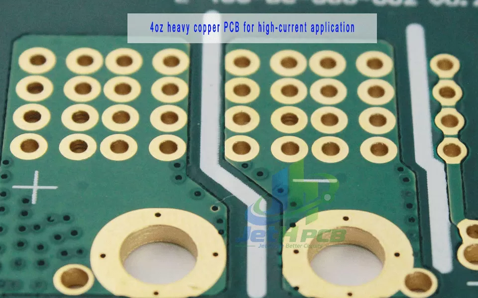
Build high-current PCB designs around manufacturable copper weights, trace geometries, multilayer stackups, vias, and terminal connections.
JetH Pro PCB Fab provides custom heavy copper PCB manufacturing for power electronics, battery systems, motor drives, industrial power supplies, charging equipment, and other applications with demanding current and temperature-rise requirements.
ENGINEERING DEFINITION
Heavy Copper Is More Than a Higher Copper Weight
A heavy copper PCB uses thicker copper conductors than a conventional PCB to support high-current paths, control conductor temperature rise, improve power distribution, or reinforce selected electrical connections.
Heavy copper capability should not be evaluated by maximum copper weight alone. A valid capability assessment must connect requested copper thickness with layer count, trace geometry, hole structure, board thickness, and finished tolerances.
*Maximum values apply to selected prototype and low-volume constructions. Final capability depends on copper distribution, layer count, board thickness, hole structure, design geometry, and production quantity.
Power distribution and moderately high-current paths.
Higher current with moderate layout density.
Heavy copper power and control boards.
High-current power boards.
Highly demanding current paths.
Two traces using the same copper weight can have very different current-carrying capabilities if their widths, lengths, layer positions, or cooling conditions are different.
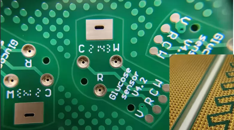
Increasing copper thickness changes how the PCB must be designed and manufactured.
It affects more than conductor resistance.
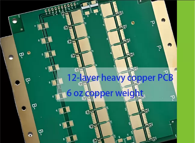
Thicker copper requires deeper etching. As copper weight increases, lateral etching and conductor-shape control become more difficult.
A wide, heavy copper conductor may narrow abruptly as it reaches a small component pad. This can create a current bottleneck, greater etching sensitivity, pad-shape distortion, and uneven heat transfer during soldering.
Heavy inner-layer copper creates greater height differences. The stackup must provide enough resin flow without voids or resin starvation.
Large, unbalanced copper areas can affect lamination behavior, dimensional stability, and board flatness.
Heavy copper may need to remain on selected power regions while signal routing uses another copper construction.
Via count, finished hole size, hole copper, pad diameter, and current distribution between layers must also be evaluated.
Base copper is the nominal copper thickness of the copper-clad material before subsequent outer-layer plating and processing.
Finished copper is the resulting conductor thickness after relevant manufacturing processes. On outer layers, it may include electroplated copper.
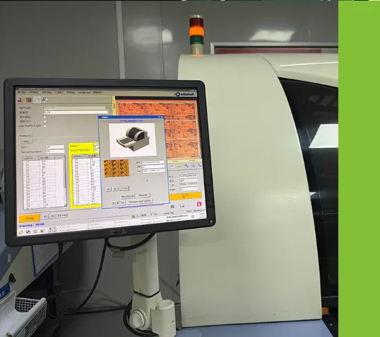
Heavy copper capability should be supported by measurable production and inspection controls.
Material Verification / Etching / AOI / Electrical Test / Microsection / Lot Traceability
Heavy copper increases thermal mass around pads, terminals, and power components.
Thermal relief can improve solderability, but an overly restricted connection may reduce current capacity. The connection must balance electrical, thermal, and assembly requirements.
There is no universal heavy-copper reflow profile. The correct profile depends on board size and thickness, copper distribution, component thermal mass, solder paste, component limits, oven performance, and measured board temperatures.
Charging, discharging, contactor control and terminals.
Power switching and phase-current paths.
Distribution, protection and high-current interfaces.
Battery interfaces and inverter systems.

Copper requirements reviewed layer by layer.
Geometry, spacing, vias, stackup and copper balance reviewed before fabrication.
Base copper, finished copper, tolerance and inspection requirements clarified.
If your copper weight or stackup has not been finalized, provide current requirements, available routing area, board dimensions, and expected operating conditions for preliminary engineering review.
There is no single threshold used by every manufacturer. For manufacturing, it is more important to define copper requirements for every layer, distinguish base copper from finished copper, and confirm corresponding trace and spacing limits.
A 4 oz copper weight does not have one fixed current rating. Trace width, length, layer placement, temperature rise, parallel layers, vias, terminals and cooling conditions must also be considered.
Minimum trace and spacing depend on copper thickness, layer location, conductor tolerance, pattern density and fabrication process. Thicker copper generally requires wider traces and larger spacing.
Base copper is the nominal thickness of the starting copper-clad material. Finished copper is the resulting conductor thickness after applicable processing and plating.
Provide Gerber or ODB++ data, drill files, stackup, copper weight for every layer, base or finished copper requirements, board thickness, material, surface finish, quantity, inspection requirements, and relevant current and temperature-rise conditions.
Send your Gerber files, stackup, copper requirements, current conditions, and quantity for manufacturing review.
Our team will get back to you within 24 hours
 DFM & Design Review
 Technical Consultation
 Fast Response
 中文