

 中文
When to Use Via-in-Pad in HDI PCB Design
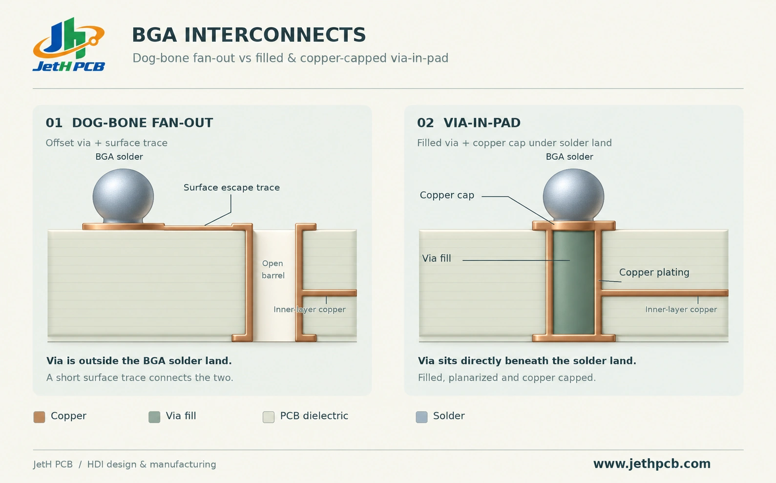
Via-in-pad places a via directly inside a component’s solder land. It can open escape-routing channels, shorten interconnects and connect thermal pads to copper planes. The right choice depends on the package, stack-up, electrical requirements and manufacturing process—not BGA pitch alone.
When Routing Density Justifies Via-in-Pad
At fine BGA pitches, the challenge is the usable copper channel between lands and via pads. Ball pitch, land diameter, solder-mask clearance, drill registration and trace spacing all consume that channel. A smaller pitch therefore makes via-in-pad more attractive, but does not automatically make it necessary.
For one trace between two equal circular pads, a first geometric check is pitch − pad diameter ≥ trace width + 2 × copper clearance. This simplified check excludes fabrication tolerances and diagonal escape geometry. The final layout must also pass drill-to-copper, annular-ring and assembly checks.
TI’s TM4C123x guide provides a useful counterexample to a universal pitch rule: its selected 0.65 mm BGA ball map permits routing on a four-layer board. Package-specific guidance should take priority over a generic pitch threshold.
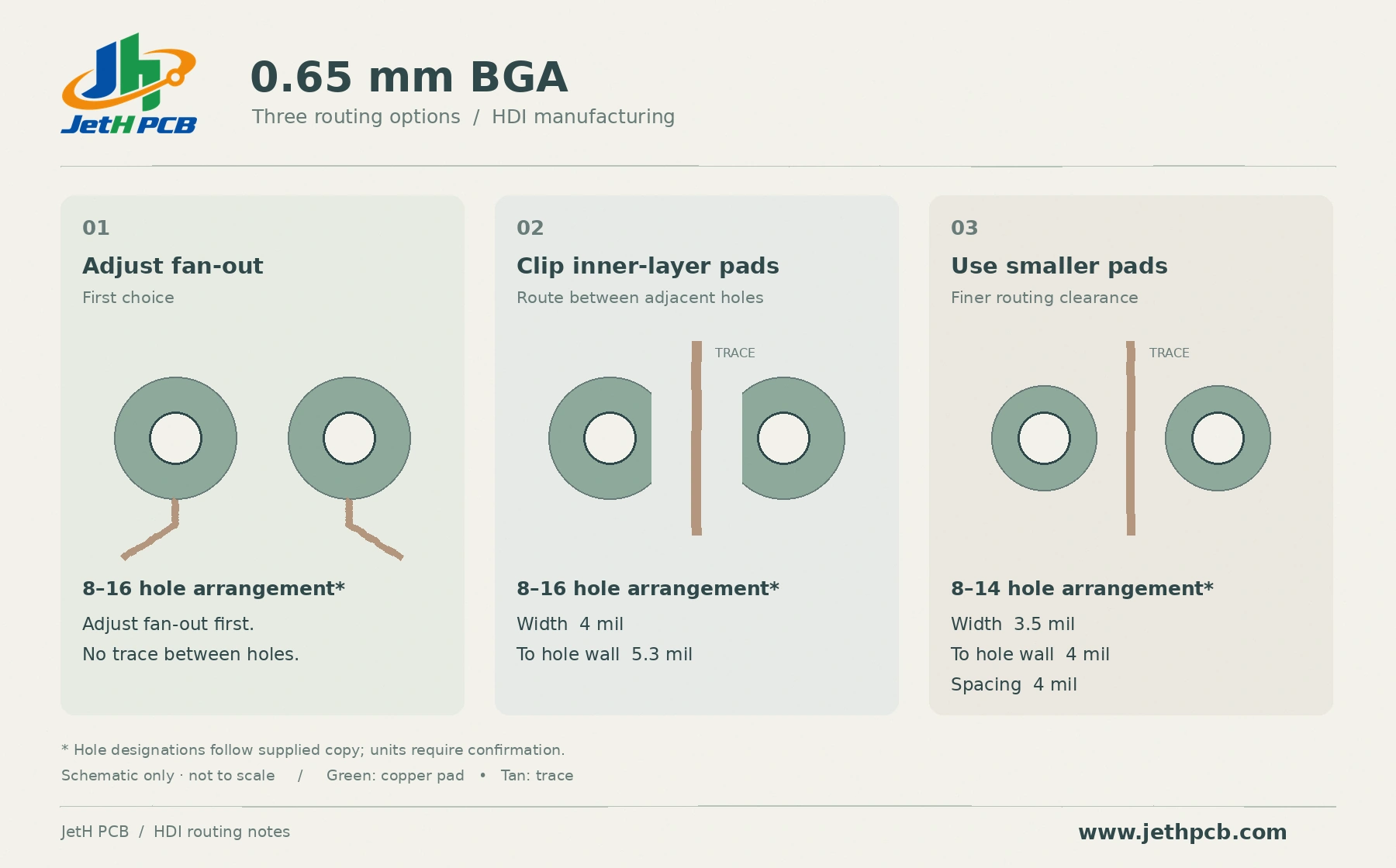
Three JetH PCB Routing Options for a 0.65 mm BGA
| Routing option | Starting dimensions | Engineering review |
|---|---|---|
| Adjust fan-out first | 8–16 designation* | Use when no trace is needed between adjacent holes. |
| Clip inner-layer via pads | 8–16 designation*; 4 mil trace; 5.3 mil trace-to-hole-wall clearance | Confirm pad modification, registration allowance and clearance on each affected layer. |
| Use a smaller via-pad arrangement | 8–14 designation*; 3.5 mil trace; 4 mil spacing; 4 mil trace-to-hole-wall clearance | Confirm the annular ring and production process window before release. |
* The supplied 8–16 and 8–14 designations need confirmation of units and drill/pad meaning. They are not interpreted here as millimetres. These are project review inputs, not universal manufacturing limits. 1 mil = 0.0254 mm.
For package escape planning and stack-up discussions, explore JetH PCB’s HDI PCB for BGA manufacturing support.
Signal Integrity: Shorter Paths and Controlled Transitions
A shorter fan-out can reduce interconnect length, but via-in-pad does not automatically remove a through-via stub. The unused barrel remains unless the design uses an appropriate blind via, microvia or backdrilled structure. Assess the signal via, reference planes and nearby return vias together.
Impedance changes can reflect energy; interrupted reference planes can force return current around a larger loop. For fast interfaces, compare transition geometry and the signal’s edge rate rather than relying on one frequency or data-rate threshold. Pad size, antipad clearance, via length and dielectric spacing determine the transition’s parasitics.
Thermal Performance and Power Delivery
Thermal vias need a complete heat path
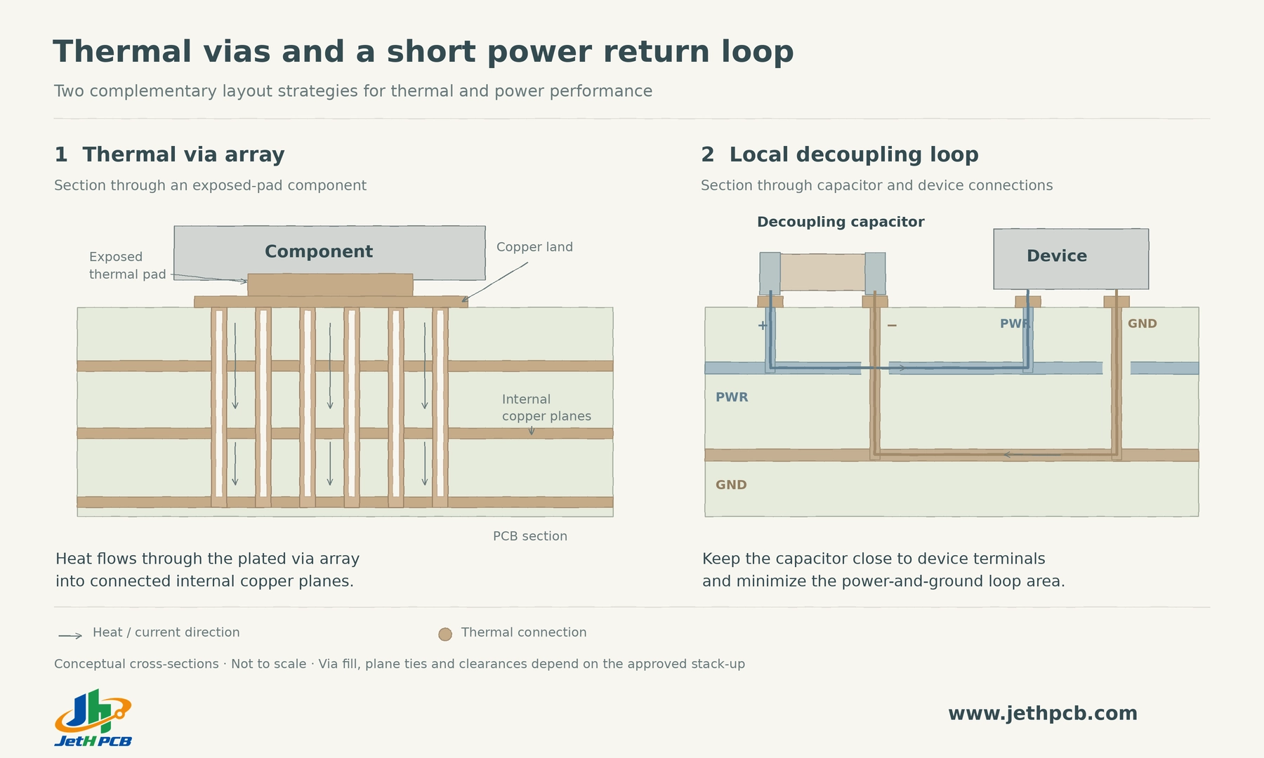
Thermal vias conduct heat from an exposed pad into connected copper layers. More parallel paths can lower the via array’s thermal resistance, but copper spreading and heat transfer to the air still limit the complete system. Pad solder coverage, board area, airflow and enclosure conditions affect junction temperature.
Follow the component’s thermal-land and assembly recommendations. Resin filling and solid copper filling are different processes; do not assume they have the same thermal conductivity. An unfilled thermal via can also draw solder away from the joint, so its opening and treatment must be coordinated with the stencil and reflow process.
Power vias must satisfy DC and transient requirements
For a DC path, voltage drop is V = I × R. An illustrative 0.9 mΩ path carrying 100 A would drop 90 mV and dissipate 9 W; this is not a recommended current rating for one via. Parallel vias need adequate plane connections, copper thickness and current-sharing margin.
For a changing load, ΔV = L × dI/dt. A 1 nH loop at 1 A/ns produces a 1 V inductive drop. Via-in-pad can shorten part of a decoupling loop, but the package, capacitor, planes and return connections remain. Adding capacitors alone does not guarantee the target impedance because shared inductance and resonances also matter.
Via-in-Pad vs Dog-Bone: Cost and Manufacturing Trade-offs
A blind microvia connecting L1 to L2 leaves deeper routing layers free of that via’s barrel and associated clearance. This can improve routing density. Via-in-pad itself does not guarantee fewer layers: the benefit comes from the full escape pattern and stack-up.
Compare total fabricated-board cost, including sequential lamination, laser drilling, filling, copper capping, planarization, inspection and yield. A lower layer count may offset some extra processing, but there is no universal layer-count crossover or fixed HDI premium.
For a geometric comparison, a circular 6 mil pad has an area of about 28.3 mil², while a 24 mil pad has an area of about 452.4 mil². That is a 93.75% reduction in pad copper area—not a board-area saving. Actual routing occupancy also includes clearance and capture-pad requirements.
When Conventional Fan-out Is the Better Fit
- Routing space is sufficient: A dog-bone escape may meet the requirements with fewer processing steps.
- Small solder lands are sensitive to paste loss: Keep open vias away from solderable pads unless an approved filling or assembly process controls solder wicking.
- Via geometry exceeds the process window: Review drill diameter, depth, plating and filling separately for through vias and laser microvias. Board thickness alone does not establish feasibility.
- The via is outside the soldering area: Filling and copper capping may be unnecessary unless another requirement calls for them.
A Practical BGA Fan-out Decision Checklist
- Check the package land pattern, ball map and recommended escape routing.
- Define trace width, copper clearance, drill-to-copper clearance and registration allowances separately.
- Select via start and stop layers, drill sizes, capture pads and the HDI build-up sequence.
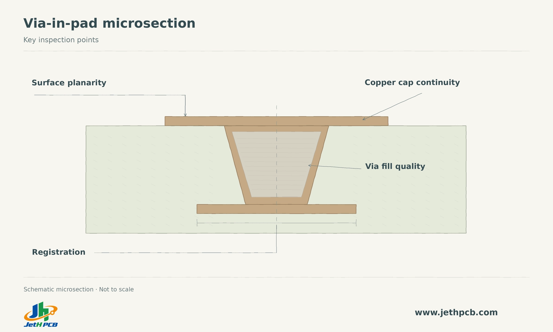
- Specify fill material, copper cap and finished pad planarity wherever the via lies in a solder joint.
- Review signal transitions, return paths, power impedance and thermal performance.
- Agree on fabrication tolerances, inspection and applicable IPC design, qualification and acceptance requirements before release.
Use conventional fan-out where it meets the requirements. Use via-in-pad where routing density or performance benefits justify the process, and confirm the design with the fabricator and assembler before production.
Technical References
- Ken Krakow, Sheldon Johnson, Jonathan Guy — System Design Guidelines for the TM4C123x Family of Tiva™ C Series Microcontrollers
- Alexander Weiler, Alexander Pakosta, Ankur Verma — High-Speed Layout Guidelines
- Steven Kummerl — PowerPAD™ Thermally Enhanced Package
- Texas Instruments — AN-2020 Thermal Design By Insight, Not Hindsight