
 中文
When comparing RF PCB suppliers, buyers often encounter similar claims about Rogers and PTFE materials, high-frequency capability, and controlled impedance. What is less clear is which manufacturing variables a supplier controls, what tolerances it can hold, and how it verifies the finished board. Material names alone do not establish manufacturing capability.
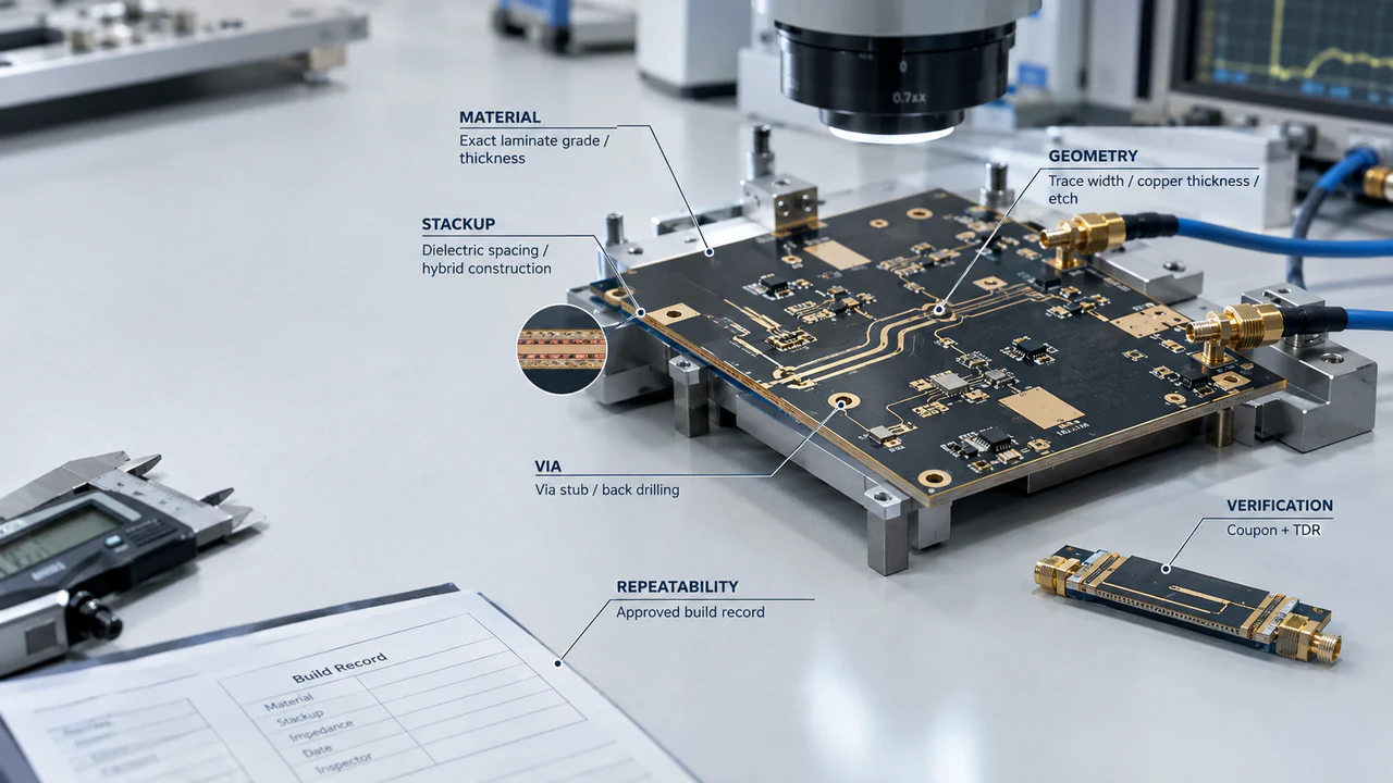
This distinction matters because RF performance depends on the board as built, not simply on the nominal design. Differences between modeled and as-built dielectric thickness, trace geometry, copper roughness, plating, and via-stub length can cause measured impedance or loss to differ from simulation. The more useful question is not simply "Do you support Rogers?" but "What do you control, and what can you prove?" This guide breaks the evaluation into six links — material → stackup → geometry → fabrication → verification → repeatability — outlining the questions to ask and the records to request at each stage.
What an RF PCB Supplier Actually Controls
Walk the same chain the signal walks:
| Link in the chain | What the supplier must control | What you should ask to see |
|---|---|---|
| Material | Exact laminate grade, thickness, copper foil type, storage and handling | Datasheet match, lot traceability |
| Stackup | Layer arrangement, dielectric spacing, bonding system, hybrid construction | Controlled stackup record, calculation basis |
| Geometry | Line width/space, etch profile, plating thickness | Finished geometry, cross-sections |
| Fabrication | Lamination, drilling, plating, surface finish, registration | Process records, capability limits |
| Verification | Impedance measurement, microsection, electrical test, PIM where relevant | Coupon + TDR reports, test records |
| Repeatability | Version-controlled build record applied to repeat orders | Approved baseline and change history |
Don't ask only what a supplier can make — ask what variable each step controls, what tolerance it qualifies, and what evidence it provides. The sections below expand each link into concrete evaluation criteria. For an overview of how we manufacture these boards, see RF & Microwave PCB.
RF PCB Materials: Verify the Grade, Not the Brand
"Rogers PCB" is not a specification. The same brand family spans materials with very different electrical behavior, processing requirements, and cost. A qualified RF PCB manufacturer will talk about the exact grade first. The common material systems are:
| Material system | Typical grades | Dk (process) | Df @ 10 GHz | Processing profile | Typical fit |
|---|---|---|---|---|---|
| Hydrocarbon/ceramic | RO4003C | 3.38 ± 0.05 | 0.0027 | Processes like FR-4, no special via treatment | Low-loss multilayer, volume production |
| Hydrocarbon/ceramic | RO4350B | 3.48 ± 0.05 | 0.0037 | Flame-retardant, FR-4-like processing | Mainstream RF builds, mixed digital/RF |
| PTFE/glass microfiber | RT/duroid 5880 | 2.20 ± 0.02 | 0.0009 | PTFE handling; sensitive to drill/plating parameters | Broadband, low-loss RF and microwave circuits |
| Low-loss glass laminate | Isola I-Tera MT40 (RF/MW) | 3.38 / 3.45 / 3.60 / 3.75, depending on construction | 0.0028–0.0035 | Standard processing, no special via treatment | Cost-effective PTFE alternative, multilayer |
Values are laminate-maker datasheet figures — RO4003C/RO4350B, RT/duroid 5880, and I-Tera MT40 — specified at defined test frequencies and methods. Rogers itself lists a different process Dk for 4 mil RO4350B (3.33 ± 0.05 instead of the typical 3.48 ± 0.05), so confirm the exact laminate thickness rather than inferring its dielectric properties from a typical material value. These figures are design references, not guaranteed finished-board constants.
Four checks separate a material-capable supplier from one that only lists brands:
- Exact grade, thickness, and foil. "We support Rogers" is not the same as stocking your grade in your laminate thickness with the right copper foil. Ask the supplier to confirm grade + thickness + foil type in the quote, not just the brand.
- Which Dk the stackup calculation uses. Laminate makers distinguish process Dk (the datasheet value) from design Dk recommended for impedance modeling — for RO4003C, process Dk is 3.38 while design Dk is 3.55. A supplier that cannot say which value its stackup calculation uses will struggle to hit your tolerance.
- PTFE handling experience. PTFE laminates reward you with very low loss and punish unprepared processes: drilling parameters, hole preparation, and lamination all differ from FR-4 practice. Ask how the supplier qualifies PTFE builds, not whether the website lists "Teflon PCB."
- The low-loss tradeoff. Lower Df is not automatically better. Lower-loss materials can cost more and may require more specialized material handling and process control. The best choice balances electrical performance, manufacturability, availability, reliability, and cost — and for many products the practical answer is a hybrid build — see below — rather than an all-PTFE stackup.
Stackup and Impedance: From a Target Number to a Verified Result
50 Ω is a common characteristic impedance target in RF systems, but the required impedance depends on the interface and the system design — antenna feeds, filters, and power amplifier matching networks each define their own targets. A capable supplier treats impedance as a per-net requirement, not a board-level slogan, and knows that the same nominal impedance can require different trace geometries on different stackups.
What actually sets the impedance of a controlled line is the complete construction: trace width, dielectric thickness (core and prepreg), finished copper thickness, copper roughness, reference plane geometry, and — for surface microstrip — solder mask and air gaps. That has two procurement consequences:
- Impedance tolerance must be defined per net class, stackup, and verification method. Be careful with suppliers that quote a single tolerance — "±5% impedance" — for every board. Whether a tolerance is achievable depends on the specific construction, and TI's mmWave radar PCB guide explicitly recommends confirming absolute tolerance limits through simulation and margin studies rather than assuming a universal figure (TI SPRACG5).
- Calculation is not verification. Ask two separate questions: how is impedance calculated (which tool, which Dk), and how is the finished board verified? A common way to verify controlled impedance is TDR measurement on a representative coupon built into the production panel; when impedance is specified as an acceptance criterion, the measurement can be performed per IPC-TM-650 2.5.5.7, Revision A. If a supplier only offers a calculation report, the acceptance criteria are not yet defined.
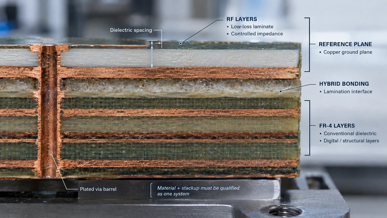
Hybrid builds deserve special attention. Mixed constructions — low-loss RF layers bonded to conventional FR-4 — are a common way to balance RF performance and material cost. They are also more than "put Rogers on one layer and FR-4 on another": the bonding system, registration between dissimilar materials, lamination cycle, and thermal behavior must be engineered as a system. TI's own mmWave radar reference designs use exactly this construction (RO4835 RF layers over an FR-4 stack). Ask a prospective hybrid PCB supplier how they qualify the lamination, not just whether they offer it.
Fabrication Tolerances That Move RF Performance
This is the section most supplier websites go quiet on — and the one that best separates an RF-capable fabricator from a general-purpose one. TI's manufacturing guide lists the process variables that shift RF performance: substrate thickness, metal thickness, metal roughness, plating, via placement, etch tolerances, air gaps, solder mask, and layer registration. In practice, five of them deserve direct questions at RFQ stage:
Trace etching. An RF trace is not a mechanical dimension with an electrical role — its manufactured geometry is part of the electrical parameter. Line width, together with dielectric thickness and copper thickness, affects impedance, while the etch profile and lateral undercut determine how closely the finished conductor matches the intended geometry. Most suppliers can quote a line-width tolerance; fewer define and report etch factor or undercut — and definitions vary between CAM and simulation tools. Ask how the supplier defines, controls, and verifies etch factor, rather than assuming the term means the same thing everywhere.
Copper roughness. At higher frequencies, current is confined increasingly close to the conductor surface, so copper profile becomes part of the RF loss budget. TI's mmWave PCB guidance notes that rolled copper generally provides lower surface roughness — and therefore lower loss — than electrodeposited (ED) copper. Also be precise about base vs. finished copper on your drawing; if that distinction is new to you, see PCB Copper Thickness Explained.
Surface finish. Surface finish can become part of the RF loss budget at high frequencies. TI's mmWave PCB guidance specifically identifies ENIG as a poor choice for its mmWave boards because of higher loss, and uses immersion silver as a lower-loss alternative. The right finish still depends on frequency, assembly, reliability, and cost — for tight loss budgets, ask which finish options your supplier offers at your frequency band, or budget the finish penalty deliberately in the link margin instead of discovering it in the field.
Via stubs and back drilling. A plated through-hole used as a layer transition leaves a stub below the last used layer. A stub can become electrically significant as frequency rises, adding a discontinuity that shows up in insertion and return loss. Where the simulated or measured loss budget requires it, back drilling removes part of the remaining stub — ask what residual stub length the supplier controls to and how it is verified.
Dielectric thickness and registration. Impedance depends on dielectric spacing, so lamination flow control and layer-to-layer registration are electrical parameters. This is why a well-equipped facility — with controlled lamination cycles and capable inspection — is part of RF capability, not a separate concern.
No supplier should promise one universal tolerance for all of these. The professional answer sounds like: "here is the tolerance we qualify for this construction, at sample stage and at production, and here is how each is verified."
Testing and Verification: How a Supplier Proves the Build
For high-frequency and microwave printed boards, IPC-6018 provides a dedicated qualification and performance framework — which class and criteria apply still follows your product and customer requirements. The practical question for procurement is narrower: what does the supplier actually measure, on what, and what report do you receive?
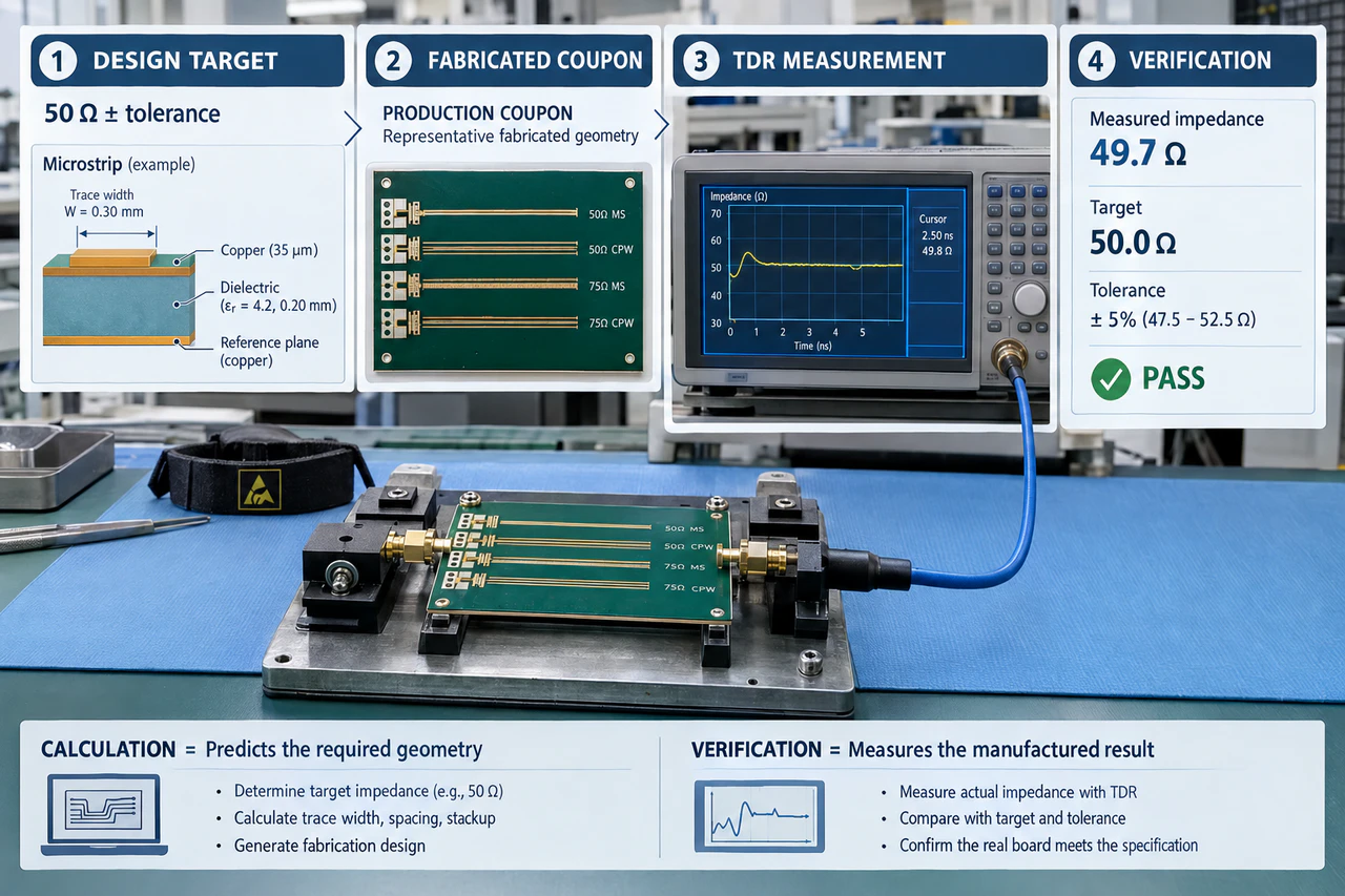
A quality promise is not a test plan. For an RF PCB, ask:
- Impedance coupon + TDR. For builds where controlled impedance is a defined acceptance criterion, ask for a representative impedance coupon on the production panel, with TDR measurement reported against your target and tolerance — not just "impedance ok." IPC-TM-650 2.5.5.7, Revision A provides a standard method for measuring characteristic impedance by TDR.
- Microsection. A destructive cross-section of a representative board section or test coupon can verify dielectric thickness, copper thickness, plating structure, and layer registration. For RF builds, the microsection is the physical proof that the stackup record was built.
- VNA / S-parameter testing. Not every project needs it, and requiring VNA testing for every build may be unnecessary. For projects with explicit RF electrical acceptance criteria, VNA-based verification can be specified and performed against those criteria.
- PIM testing where specified. For antenna, combiner, and base-station RF front-end products where passive intermodulation is a specified requirement, testing can be performed according to the applicable IEC 62037 procedures. Many capable-looking fabricators cannot test PIM at all — if your product needs it, ask for the test bands, carrier power, and limits in writing. PIM is not a universal requirement for every RF PCB; it matters where the end product has a defined passive-intermodulation limit.
- Documentation. Laminate lot traceability, material certificates, and test reports archived with the build record — so the evidence survives past shipment.
Prototype to Production: What Must Stay Consistent
The first RF lot validates the manufacturing build; every later lot must reproduce the approved record. Before committing to a supplier, ask how that record is preserved: approved material and grade, the exact stackup, fabrication data, and acceptance criteria should be version-controlled, and repeat orders should be built against that version — with any proposed change flagged for review rather than silently "improved."
This is also the right moment to ask which capability applies at which stage. Many parameters hold tighter on sample lots than in volume production; a supplier who knows its own numbers will answer precisely, e.g., "impedance is qualified at ±5% on sample builds and ±8% in production for this net class." Vagueness here is a predictor of drift later.
For overseas buyers evaluating a China-based RF PCB supplier, the same evidence rule applies to logistics: run a sample-first qualification before production quantities, confirm who your engineering contact is, and check that quotations, stackup records, and test reports arrive in English with unambiguous version control. Communication quality at RFQ stage is evidence of engineering discipline: a capable supplier identifies ambiguities, states assumptions, and documents proposed process limits before production.
Commercial fit matters too. Prototype and production lead times, minimum order requirements, available capacity, applicable quality certifications, material-change notification, and the approval process for substitutions do not change the RF design directly — but they determine whether a technically capable supplier can support the program over time.
What to Include in an RF PCB RFQ
The fastest way to filter suppliers is to send an RFQ detailed enough that only a capable one can answer it completely:
- Gerber or ODB++ data with drill files
- Proposed stackup (or ask the supplier to propose one, stating the calculation basis)
- Exact laminate grade, thickness, and copper foil; acceptable alternates
- Operating frequency or band
- Impedance targets and tolerances, per net class
- Via structures: back drilling, filled and capped vias (POFV), aspect ratios
- Surface finish
- Quantity split: sample quantity, then production forecast
- Test requirements: impedance coupon/TDR, microsection, VNA or PIM where applicable
The response itself is evidence. A capable RF PCB supplier will push back on ambiguities, propose a manufacturable stackup, and state its tolerances — before quoting. A response that repeats your RFQ back with a price tells you what the build record will look like later.
RF PCB Supplier Evaluation Checklist
Public ratings and testimonials can be useful secondary signals, but they should not replace build-specific evidence such as stackup records, impedance data, inspection reports, and traceability.
| Ask the supplier | Why it matters |
|---|---|
| Can you process the exact laminate grade, thickness, and foil? | "Supports Rogers" ≠ supports your Rogers |
| Can you build hybrid RF/FR-4 stackups, and how do you qualify the lamination? | Hybrid is a common cost/performance approach |
| Which Dk do your impedance calculations use? | Process Dk vs. design Dk errors propagate into every trace |
| How is impedance verified — coupon TDR per IPC-TM-650 2.5.5.7, Revision A? | Calculation is not acceptance |
| What impedance tolerance do you qualify, at sample and production stage? | One universal number is a red flag |
| What finished-line tolerance and etch factor do you hold? | Trace geometry is the electrical parameter |
| How are copper roughness, plating, and surface finish controlled for loss? | Conductor loss grows with frequency |
| What residual stub length do you control with back drilling? | Via stubs become electrically significant as frequency rises |
| Can you test PIM, and at which bands? | Antenna/base-station acceptance requirement |
| What reports ship with the board? | Evidence must survive past shipment |
| How is the approved stackup preserved for repeat orders? | Prevents silent drift in production |
JetH PCB: RF PCB Manufacturing Capabilities
JetH PCB manufactures custom RF and microwave PCBs — including Rogers PCB, PTFE PCB, and hydrocarbon/PPO laminates — from prototype through low-to-mid volume production. The parameters below are the ones this article says to ask for, stated in writing:
| Parameter | Production | Sample (prototype) |
|---|---|---|
| Controlled-impedance tolerance, nets ≥ 50 Ω | ±8% | ±5% |
| Controlled-impedance tolerance, nets < 50 Ω | ±4.5 Ω | ±3 Ω |
| RF line width/space etch tolerance | ±38 µm (±1.5 mil) | ±20 µm (±0.8 mil) |
| Etch factor / undercut | >5* | >8* |
| PIM (third-order passive intermodulation) | ≤ −117 dBm avg.** | ≤ −118 dBm avg.** |
| PIM test bands | 800 / 2100 / 2600 MHz bands | per customer requirement |
| Back-drill residual stub | 2–10 mil | 2–8 mil |
| Minimum mechanical drill diameter (through-hole) | 0.15 mm | 0.10 mm |
* Listed by parameter, not as one guaranteed combination on a single board. Etch factor is reported per JetH's internal process definition and varies with copper thickness and construction. Final capability depends on the selected laminate, stackup, board construction, and drawing review — tighter targets are evaluated per project.
** PIM results depend on the test configuration: the dBm figure is absolute, while the equivalent dBc value (−160 / −161 dBc) is referenced to single-carrier power at 2 × 43 dBm carriers. Confirm test power, frequencies, and measurement method when specifying PIM acceptance.
Supporting capabilities behind those numbers: hybrid lamination of RF laminates with FR-4, resin-filled and capped vias (POFV/VIPPO), ENIG/ENEPIG/immersion-tin/OSP and other finish options, and laminates sourced from major makers including Rogers, Shengyi, Nanya, TUC, Panasonic, and Doosan. Impedance builds are verified with coupons and TDR, and PIM is tested in-house at the bands above.
Where RF meets power: PA and high-power RF stages often need heavy local copper or a metal base alongside RF-controlled regions — see Heavy Copper PCB for the combined constructions. For prototype-stage qualification, JetH runs the sample-first flow described above; details in Low Volume & Prototyping.
FAQ
What is the difference between an RF PCB supplier and an RF PCB manufacturer?
A manufacturer directly performs or controls the fabrication process — including lamination, etching, plating, drilling, and testing. A supplier may be the manufacturer or an intermediary. When qualifying either, confirm who controls the process and who performs impedance and reliability verification, and ask for evidence from the fabrication floor rather than reseller documentation.
Is FR-4 acceptable for RF PCBs?
It depends on frequency and loss budget. Standard FR-4 has higher and less predictable Dk/Df than engineered RF laminates, which matters more as frequency rises. For many products the practical answer is a hybrid build: low-loss RF material for controlled-impedance layers, FR-4 for the rest.
What impedance tolerance is realistic for an RF PCB?
It must be defined per net, stackup, and verification method — no single number applies to every board. Ask which tolerance the supplier qualifies at sample stage and which applies to production, and, where impedance is an acceptance criterion, require coupon TDR measurement per IPC-TM-650 2.5.5.7, Revision A.
Does surface finish affect RF PCB performance?
Yes — surface finish can be part of the RF loss budget at high frequencies. TI's mmWave PCB guidance, for example, identifies ENIG as a poor choice for its mmWave boards because of higher loss and uses lower-loss alternatives. Discuss finish options for your frequency band with your supplier, or budget the finish penalty deliberately.
What documents should I require from an RF PCB supplier?
At minimum: the controlled stackup record, impedance coupon results with TDR values, microsection reports, laminate lot traceability or manufacturer certificates, and — for antenna and base-station products — PIM test data at your specified bands.
Have an RF PCB Build to Evaluate?
Send JetH PCB the material specification, stackup, impedance requirements, and quantities — our engineering team reviews the build against the criteria in this guide and responds within 24 hours with DFM feedback and a quotation.
Request an RF PCB Quote | See Manufacturing Facilities | Contact Us