
 中文
Quick Reference
- 1 oz: approximately 35 µm (1.37 mil) nominal copper thickness
- 2 oz: approximately 70 µm (2.74 mil)
- 3 oz: approximately 105 µm (4.13 mil)
- 20 oz: approximately 700 µm (27.56 mil)
Who this guide is for: Engineers, procurement specialists, and PCB buyers who need to interpret copper weight specifications, understand current and thermal requirements, and communicate precise copper thickness requirements to PCB manufacturers.
For engineers and PCB buyers, a copper specification such as "1 oz," "2 oz," or "3 oz" on a fabrication drawing often raises a practical question: what does that number actually mean for the finished board, current capacity, manufacturability, and the fabrication quote? A "2 oz" requirement could refer to base copper or finished copper, may or may not apply to every layer, and does not linearly double the current capacity of 1 oz — yet these distinctions are rarely explained on the drawing itself.
This guide helps you move from seeing a copper weight specification to forming a precise, manufacturable PCB copper requirement. It covers what copper weight means in micrometers, how thickness relates to current and temperature rise, when heavy copper is justified, what manufacturing trade-offs it introduces, and how to specify copper correctly when ordering — with a focus on specification and procurement rather than trace width calculation or layout design.
- What Is PCB Copper Thickness?
- PCB Copper Thickness Chart: 1 oz to 20 oz
- How Copper Thickness Affects Current and Temperature Rise
- When Should You Use Heavy Copper PCB?
- What Changes When Copper Gets Thicker?
- Can a Multilayer PCB Use Different Copper Weights?
- How to Specify Copper Thickness When Ordering a PCB
- Key Takeaways
What Is PCB Copper Thickness?
PCB copper thickness describes the thickness of the copper foil laminated onto each layer of a printed circuit board. The industry measures this indirectly as copper weight — the mass of copper per unit area, expressed in ounces per square foot (oz/ft²). One ounce of copper spread over one square foot yields a nominal thickness of approximately 34.3 µm, commonly rounded to 35 µm (1.37 mils) for practical specification.
This convention originates from the copper foil manufacturing process. Copper foil is produced by electrodepositing or rolling copper to a controlled thickness, and the area-weight specification (oz/ft²) is more directly measurable during production than a linear thickness dimension. One ounce of copper foil corresponds to a nominal thickness of approximately 34.3 µm (about 35 µm), or roughly 305 g/m². Copper weight is a common shorthand for specifying starting copper foil, while finished copper thickness may be specified separately.
Copper Weight, Base Copper, and Finished Copper
These three terms are not interchangeable, and confusing them leads to specification errors:
- Copper weight (oz/ft²) is the procurement specification — the value written on the fab drawing. It refers to the starting foil weight before processing.
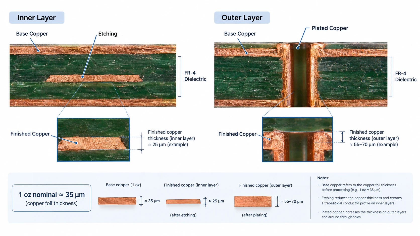
- Base copper (or starting copper) is the actual foil thickness as received from the material supplier, before any plating or etching. In conventional multilayer construction, inner-layer copper is normally etched before lamination rather than subsequently plated.
- Finished copper is the final copper thickness measured on the delivered board, after all plating and etching steps. For outer layers, plating during via formation adds copper, so finished thickness exceeds the base. For inner layers, etching reduces the thickness below the nominal starting value.
The distinction matters in practice. According to IPC-6012F, a 1 oz base copper on an inner layer yields a minimum finished thickness of only 24.9 µm after processing — not 35 µm. On external layers, plating builds copper up: 1 oz base copper produces a minimum finished thickness of 47.9 µm for Class 2 boards and 52.9 µm for Class 3. If your application requires a specific finished copper thickness, stating only "1 oz" on the drawing leaves room for interpretation.
PCB Copper Thickness Chart: 1 oz to 20 oz
The following table maps copper weight to nominal thickness in both micrometers and mils, along with typical applications for each range. These are nominal reference values — the thickness equivalent of the specified copper weight, not a guarantee of finished board thickness.
| Copper Weight | Nominal Thickness (µm) | Approx. Thickness (mil) | Typical Use |
|---|---|---|---|
| 0.5 oz | 17.5 | 0.69 | Fine-pitch signal layers, controlled impedance |
| 1 oz | 35 | 1.37 | Standard PCB, general signal and moderate power |
| 2 oz | 70 | 2.74 | Higher-current power distribution, thermal management |
| 3 oz | 105 | 4.13 | Heavy copper, power electronics |
| 4 oz | 140 | 5.51 | High-current power paths |
| 6 oz | 210 | 8.27 | Motor drives, converters, industrial power |
| 8 oz | 280 | 11.02 | High-current bus bars, power modules |
| 10 oz | 350 | 13.78 | Very high-current power distribution |
| 12 oz | 420 | 16.54 | Specialized heavy-copper designs |
| 15 oz | 525 | 20.67 | Extreme copper applications |
| 20 oz | 700 | 27.56 | Extreme high-current, specialized power constructions |
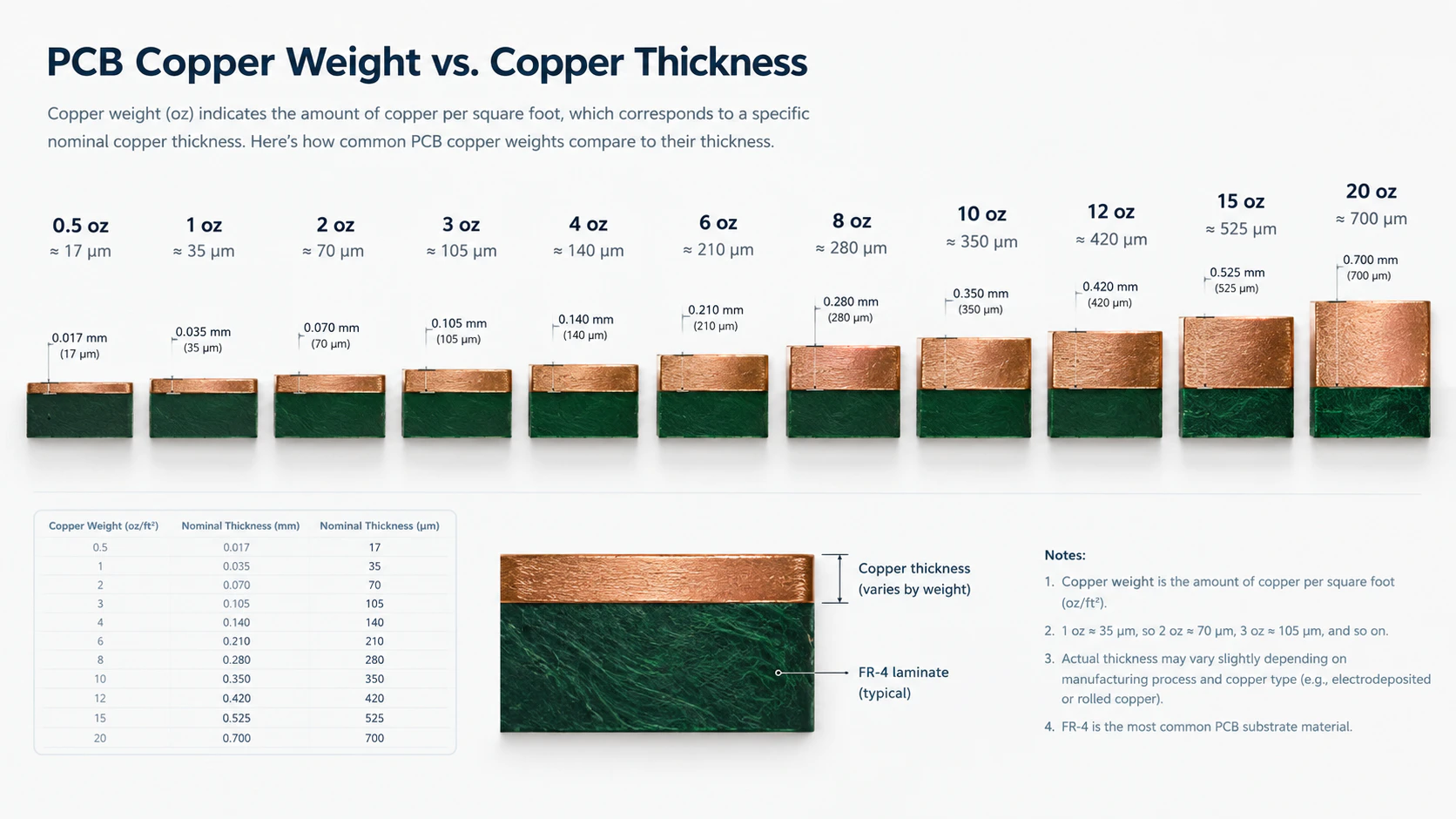
As a practical rule of thumb, each ounce of copper corresponds to roughly 35 µm of nominal foil thickness. Values from 10 oz through 20 oz are confirmed by manufacturer capability tables and represent specialized heavy copper construction rather than standard PCB offerings.
What Does 20 oz Copper Mean?
A 20 oz copper layer has a nominal thickness of approximately 700 µm (0.7 mm, 28 mil). This is far beyond conventional PCB copper — it belongs to the category of specialized high-power construction used in power distribution boards, EV charging infrastructure, and industrial power electronics. Some specialist PCB manufacturers support copper weights of 20 oz or more, but this level requires careful review of stackup, geometry, plating, and thermal requirements. A 20 oz copper PCB is not a standard production option at most PCB houses.
How Copper Thickness Affects Current and Temperature Rise
The primary reason engineers specify thicker copper is to increase current-carrying capacity. The mechanism is straightforward: thicker copper increases the cross-sectional area of a trace, reducing electrical resistance (R = ρL/A), which in turn reduces resistive heating (P = I²R) and allows more current to flow at a given temperature rise.
What is less straightforward — and frequently misstated in online resources — is that this relationship is not linear. Doubling copper thickness from 1 oz to 2 oz does not double current capacity. In a fixed-width reference example, moving from 1 oz to 2 oz increases the allowable current by roughly half rather than doubling it. For instance, a 1 oz external trace 50 mil wide at a 10°C temperature rise handles approximately 2.6 A; the same trace in 2 oz copper carries roughly 4.0 A — a meaningful increase, but far from double.
Copper Thickness vs. Current and Temperature Rise
The relationship between copper thickness and current capacity is not a simple lookup. IPC-2152 provides conductor-sizing charts that relate current, acceptable temperature rise, and conductor cross-sectional area — but these charts must be used with the specific conductor geometry, board construction, and thermal environment, not read as a universal ampacity table.
| Copper Thickness | Current-Carrying Capacity at the Same Width | Effect of Higher Allowable Temperature Rise |
|---|---|---|
| 1 oz | Reference level | Higher allowable current |
| 2 oz | Higher than 1 oz | Higher allowable current |
| 3 oz | Higher than 2 oz | Higher allowable current |
| 4 oz+ | Further increases potential capacity | Must be evaluated with the complete thermal design |
Copper thickness alone does not provide a universal ampacity rating. The actual current a trace can carry depends on trace width, layer position, board material, nearby copper planes, ambient conditions, and the allowable temperature rise — all of which IPC-2152 accounts for in its conductor-sizing charts.
Why Copper Thickness Alone Does Not Determine Current Capacity
IPC-2152, a widely referenced industry reference for relating conductor size, current, and temperature rise, accounts for multiple variables beyond copper thickness:
- Trace width — the other dimension of the conductor cross-section, equally important as thickness
- Layer position — internal vs. external layers dissipate heat differently
- Allowable temperature rise — higher ΔT permits more current at the cost of reliability
- Board thickness and material — thermal conductivity of the substrate affects heat spreading
- Nearby copper planes — solid copper planes act as heat sinks, improving capacity
- Ambient environment — air, vacuum, or enclosed conditions change heat transfer
- Board mounting — how the board is physically mounted affects convection
The older IPC-2221 standard, which many online calculators still reference, assumed internal traces carry half the current of external traces. IPC-2152 (released in 2009) showed that internal conductor temperature behavior can differ substantially from the assumptions used in older sizing charts, depending on board construction and thermal paths. This is one reason why older IPC-2221-based calculators can produce results that differ substantially from IPC-2152-based analyses, particularly for internal conductors.
For procurement purposes, the key takeaway is: do not select copper thickness based on a simple "X oz = Y amps" lookup. The current requirement, trace width, layer structure, and temperature rise limit must be considered together. If the design team has not provided this analysis, request it before specifying copper weight on the fabrication drawing.
When Should You Use Heavy Copper PCB?
Heavy copper PCB is an industry term for boards with copper thickness of approximately 3 oz/ft² (105 µm) or greater. It is worth noting that this threshold is an industry convention — no IPC standard formally defines "heavy copper" at a specific ounce value. Some manufacturers classify 2 oz and above as thick copper; others reserve "heavy copper" for 3 oz+ and use "extreme heavy copper" for 10 oz and above. The variation means buyers should state the actual copper requirement rather than relying on the label.
The table below maps copper weight ranges to typical application categories:
| Copper Weight | Typical Applications |
|---|---|
| 0.5–1 oz | General-purpose PCBs, signal layers, moderate power, controlled impedance designs |
| 2 oz | Higher-current power distribution, LED boards, thermal-demanding designs |
| 3–4 oz | Power electronics, DC-DC converters, motor drivers, automotive ECUs |
| 6–10 oz | Industrial motor drives, power inverters, EV charging, high-current bus bars |
| 12–20 oz | Extreme high-current power distribution, specialized industrial power systems |
The decision to use heavy copper is driven by current requirements that exceed what standard 1 oz copper can handle at practical trace widths. A 15 A power path may require substantially wider routing when using 1 oz copper, depending on the allowable temperature rise and thermal conditions; moving to 4 oz or 6 oz copper allows the same current at a narrower width. Heavy copper also improves heat spreading across the board, reducing localized hot spots — though it does not eliminate the need for proper thermal management, and claims that heavy copper "replaces heat sinks" are overstated.
Explore JetH's Heavy Copper PCB manufacturing capabilities for high-current and multilayer applications. JetH supports finished copper constructions up to 20 oz, subject to the specific stackup, geometry, board thickness, hole structure, and production conditions.
What Changes When Copper Gets Thicker?
Selecting heavier copper affects more than just current capacity. Every increase in copper thickness introduces manufacturing consequences that translate into design constraints and cost. Understanding these trade-offs is essential for buyers evaluating whether heavy copper is necessary for their application.
| Manufacturing Factor | Effect of Thicker Copper | Practical Consequence |
|---|---|---|
| Etching | Greater lateral etching and more difficult conductor-profile control | Minimum trace/space may need to increase |
| Plating | More demanding thickness and distribution control | Hole and surface copper requirements should be reviewed |
| Lamination | Greater copper step height | Stackup and resin flow need review |
| Drilling / Vias | Current paths and aspect ratio become more important | Hole size and via structure must match the board construction |
| Solder mask | Greater surface step height | Mask coverage and openings should be reviewed |
| Board flatness | Copper imbalance can affect dimensional stability | Stackup and copper distribution should be balanced |
| Cost | More material and process control | Cost increases as construction becomes more demanding |
Etching deserves particular attention because it is the most fundamental constraint. The etching process removes copper both vertically (to define trace thickness) and laterally (undercut, which widens gaps and narrows traces). The thicker the copper, the more pronounced the lateral etching effect, producing trapezoidal trace cross-sections and making conductor-profile control more difficult. At 3 oz and above, additional etching-process control and line-width compensation may be required to maintain the intended conductor geometry.
For controlled-impedance designs, copper thickness also affects conductor geometry and therefore the impedance target. This article focuses on copper specification and thermal considerations rather than impedance calculation; for impedance-controlled multilayer designs, copper thickness, dielectric thickness, and trace geometry should be reviewed together. See JetH's Multilayer PCB manufacturing for stackup and impedance control capabilities.
The practical implication for procurement: heavier copper generally forces wider minimum trace/space rules, which may conflict with fine-pitch component requirements. If a board combines high-current power paths with fine-pitch signal components, mixed copper weights (discussed next) may be a better approach than specifying heavy copper on every layer.
Can a Multilayer PCB Use Different Copper Weights?
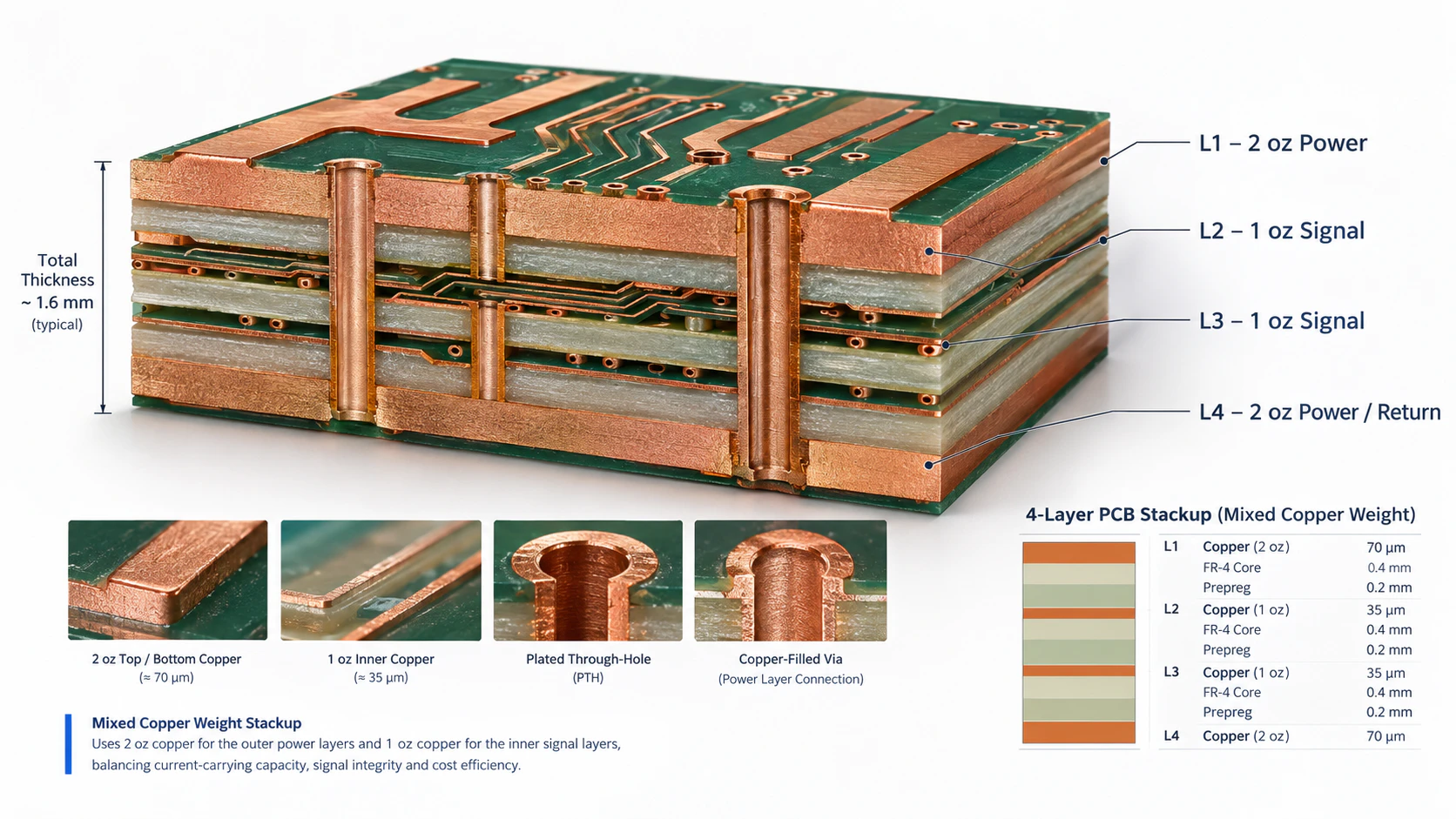
Yes — and in power electronics designs, this is common practice. A multilayer PCB can use different copper weights on different layers, allowing signal layers to use lighter copper (0.5–1 oz) for fine-pitch routing while power layers use heavier copper (2–6 oz or more) for high-current paths.
This approach, sometimes called mixed copper weight or mixed-weight stackup, lets designers optimize each layer for its function without forcing the entire board to heavy copper. A typical 4-layer configuration might be:
| Layer | Copper Weight | Function |
|---|---|---|
| L1 (Top) | 2 oz | Power routing, component pads |
| L2 (Inner) | 1 oz | Signal routing |
| L3 (Inner) | 1 oz | Signal routing |
| L4 (Bottom) | 2 oz | Power return, component pads |
For higher power designs, a 6-layer board might use 3 oz or 4 oz on dedicated power layers while keeping signal layers at 1 oz. Mixed copper can cost less than using heavy copper on every layer, but the actual premium depends on the stackup and fabrication process.
Stackup Guidance for Mixed Copper
Two considerations are important when specifying mixed copper weights:
- Matching copper weights on outer layers is a common way to improve stackup balance. The top and bottom layers do not universally have to use the same copper weight — different outer-layer weights may be possible when the fabricator's process supports the construction and copper balance is addressed.
- A balanced, symmetrical stackup is commonly preferred. Layers symmetrically positioned about the center core typically use the same copper weight to reduce the risk of board warpage. An unbalanced stackup — for example, 4 oz on top and 1 oz on bottom with asymmetric inner layers — can contribute to bow and twist during lamination and reflow.
Mixed copper is particularly relevant for designs that combine high-current power delivery with controlled-impedance signal routing. Using heavy copper on signal layers would force wider traces, changing conductor geometry and routing density. Keeping signal layers at 0.5–1 oz while allocating 2–4 oz to power layers can help balance fine-pitch routing, impedance requirements, and high-current power distribution.
How to Specify Copper Thickness When Ordering a PCB
Ambiguous copper specifications can lead to manufacturing questions, unexpected cost changes, or acceptance disputes. The guidance below covers what to include on the fabrication drawing and in the RFQ package.
What to Specify
| Parameter | Why It Matters | Common Mistake |
|---|---|---|
| Copper weight per layer | Each layer can have a different weight; defaults vary by manufacturer | Writing "heavy copper" without stating the actual oz value |
| Base copper or finished copper | Determines whether the spec refers to starting foil or post-processing thickness | Writing "3 oz copper" without clarifying base vs. finished |
| Performance class (IPC-6012 Class 2 or 3) | Class 3 requires thicker minimum finished copper, affecting cost | Not specifying class when reliability is critical |
| Trace width and spacing | Must meet minimum design rules for the specified copper weight | Specifying 3 oz copper with 4/4 mil spacing (below manufacturing capability) |
| Maximum current per net | Allows the manufacturer to review copper adequacy | Omitting current data, forcing the manufacturer to guess |
| Allowable voltage drop / resistance target | Ensures the power path meets both thermal and electrical requirements | Checking thermal ampacity but ignoring voltage drop on long power traces |
| Allowable temperature rise | Defines the thermal limit for current capacity verification | Using an unspecified or overly conservative ΔT |
| Board thickness and layer count | Affects thermal performance and manufacturability | Changing copper weight without adjusting board thickness |
| Via structure and hole requirements | Heavy copper affects drilling and plating | Specifying small vias with 6 oz+ copper |
| Surface finish | Must be compatible with thick copper step heights | Surface finish and solder-mask processes may require review when thick copper creates significant surface topography |
Specification Checklist for the Fab Drawing
- State the copper weight for every layer explicitly. Do not write "heavy copper" — write "L1: 2 oz, L2: 1 oz, L3: 1 oz, L4: 2 oz" or equivalent.
- Clarify whether the specification is base copper or finished copper. If finished copper thickness is critical to the design, state "finished copper thickness per IPC-6012, Class [2/3]."
- Include the IPC performance class. Specify the applicable IPC performance class based on customer and end-use requirements. Class 3 is intended for high-reliability applications where continued performance is critical; it is not automatically required for every aerospace, medical, or automotive PCB.
- Attach the stackup diagram showing copper weight per layer, dielectric thicknesses, and material specifications.
- Provide current and thermal data for power nets: maximum sustained current, peak current, allowable temperature rise, and allowable voltage drop or resistance target.
- List minimum geometry requirements (trace width, spacing, via diameter) that are compatible with the specified copper weight.
Many standard PCB services use 1 oz-class copper as a common starting point, but default constructions vary by manufacturer. Do not rely on an unspecified copper-weight default when the copper thickness is electrically or thermally critical.
Need Help Defining Your Copper Requirements?
If your copper weight, finished copper thickness, or stackup has not been finalized, send JetH your fabrication data for an engineering review and quotation. Request a PCB Quote.
Key Takeaways
- 1 oz copper is approximately 35 µm nominal, while finished copper thickness depends on the layer and manufacturing process.
- Copper weight and finished copper thickness are not interchangeable specifications. Specifying "1 oz" does not guarantee a 35 µm finished thickness — inner layers finish lower due to processing; outer layers finish higher due to plating.
- Higher copper thickness can increase current-carrying capability, but current depends on conductor geometry and thermal conditions — not copper weight alone. IPC-2152 provides reference charts and guidance for this relationship.
- Heavy copper has no single IPC-defined ounce threshold; 3 oz and above is a common industry convention. It is appropriate for power electronics and high-current applications, but introduces manufacturing constraints that should be reviewed with the fabricator.
- For procurement, specify copper weight or finished copper thickness per layer, applicable performance requirements, stackup, geometry, current/thermal conditions, and allowable voltage drop — never just "heavy copper" without numbers.
- The goal of this guide is practical: after reading, you should be able to turn an ambiguous requirement such as "heavy copper PCB" into a precise, layer-by-layer copper specification that a PCB manufacturer can quote and build without guesswork.
Reviewed by PCB Manufacturing Engineer · Last updated: September 2026