
 中文
When designing a custom FPGA PCB, one of the earliest and most consequential decisions is the layer count and stackup arrangement. Unlike generic digital boards, FPGA PCBs must simultaneously manage high-speed differential interfaces, dense ball grid array (BGA) packages, multiple power rails with stringent transient current demands, and—increasingly—mixed-signal integration. The stackup you choose directly impacts signal integrity, power distribution network (PDN) performance, electromagnetic compatibility (EMC), routing feasibility, and ultimately, manufacturing cost and yield.
The challenge is that there is no universal "correct" layer count for FPGA designs. A 6-layer PCB stackup may be entirely sufficient for a mid-range FPGA with moderate I/O and standard interfaces, while an 8-layer PCB stackup becomes necessary when BGA escape routing density, high-speed SerDes channels, or multiple voltage domains push beyond what six layers can reasonably accommodate. The decision should be driven by your specific FPGA device, its package, your interface requirements, and your manufacturer's capabilities—not by a blanket assumption that more layers always means better performance.
This guide provides a technical framework for making that decision, drawing on AMD/Xilinx UG583, Intel AN 315, Altium design resources, and IPC standards.
- What Makes FPGA PCB Design Unique
- 6 Layer PCB Stackup for FPGA Designs
- 8 Layer PCB Stackup for FPGA Designs
- 6 Layer vs 8 Layer PCB: Which Stackup Should You Choose?
- High-Speed PCB Design Considerations for FPGA
- BGA Escape Routing for FPGA Packages
- Choosing a Custom PCB Manufacturer for FPGA Boards
- From Design to Production: Multilayer PCB Fabrication
- Conclusion: Designing Your Custom FPGA PCB
- Request an FPGA PCB Quote
What Makes FPGA PCB Design Unique
FPGA PCB design differs from conventional digital PCB design in several critical ways:
Dense BGA Packages with Fine Pitch
Modern FPGAs use high-pin-count BGAs with pitches from 1.0 mm down to 0.4 mm and below. BGA escape routing—fanout from the solder ball array to routing channels—often becomes the primary driver of layer count. As Altium's design resources note, evaluate fanout feasibility before finalizing layer count.
Multiple Power Rails with High Transient Currents
A typical FPGA requires several distinct power domains (VCCINT, VCCIO, VCCAUX, transceiver supplies). AMD's UG583 states that high-priority power planes should be paired with adjacent ground planes to minimize parasitic loop inductance, directly constraining layer count.
High-Speed Serial Interfaces
Contemporary FPGAs implement PCIe Gen3/Gen4/Gen5, multi-gigabit transceivers, DDR4/DDR5, and links at 10–25 Gbps and beyond. These demand controlled impedance, continuous reference planes, length-matched differential pairs, and careful via transition management. Intel's AN 315 emphasizes that signals with sub-1 ns rise times must be treated as high-speed regardless of clock frequency.
Mixed-Signal Integration
FPGAs with integrated ADCs/DACs (e.g., Xilinx RFSoC) or designs with external analog front ends introduce analog/digital noise coupling and return-path management challenges, sensitive analog routing, and dedicated clean power planes—requirements that frequently push designs toward 8+ layers.
6 Layer PCB Stackup for FPGA Designs
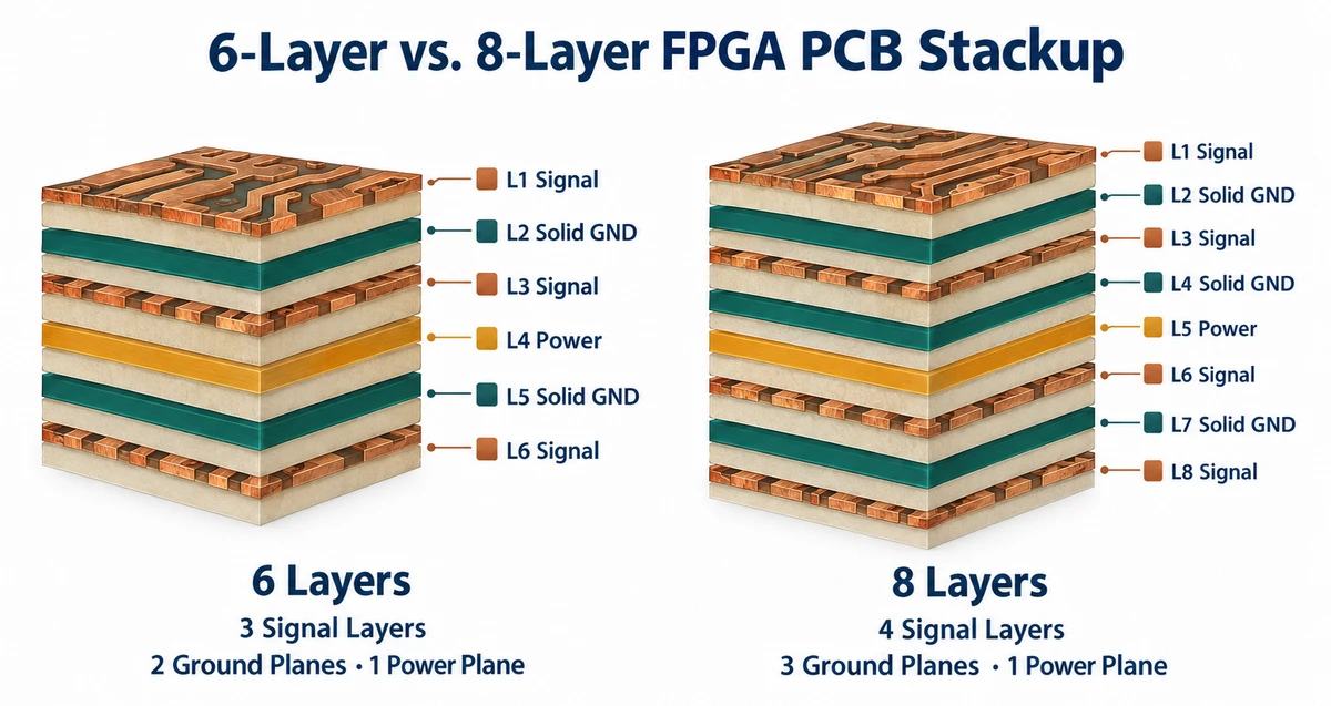
A 6-layer PCB stackup provides three signal layers, two ground planes, and one power plane (or variations thereof). For many FPGA designs—particularly those with moderate pin counts, standard interfaces (SPI, I2C, UART, gigabit Ethernet), and a manageable number of power rails—six layers can deliver excellent performance when the stackup is properly arranged. This guide focuses on designs where 6 or 8 layers are viable; large FPGA packages with high pin counts may require additional layers.
Example 6-Layer Stackup: SIG-GND-SIG-PWR-GND-SIG
One commonly used 6-layer arrangement for FPGA and high-speed digital design is:
| Layer | Function | Notes |
|---|---|---|
| L1 | Signal (Top) | Component side, BGA fanout, high-speed microstrip |
| L2 | GND (Solid) | Reference plane for L1; adjacent reference plane for L3 |
| L3 | Signal (Inner) | Stripline routing, controlled impedance |
| L4 | PWR (Plane) | Power distribution; adjacent to L3 and paired with L5 |
| L5 | GND (Solid) | Reference plane for L6; adjacent to L4 |
| L6 | Signal (Bottom) | Routing, passive components |
Key advantages:
- Every signal layer (L1, L3, L6) has an adjacent solid ground reference plane, enabling controlled impedance and predictable return current paths.
- The power plane (L4) is tightly coupled with the ground plane (L5), creating a distributed plane capacitor that improves PDN high-frequency response.
- Two solid ground planes provide effective EMI shielding and low ground impedance.
Limitations to evaluate:
- Only three routing layers (L1, L3, L6). For dense BGA packages, this may be insufficient for complete escape routing.
- A single power plane may require plane splitting if the FPGA has multiple voltage domains, which can degrade return path continuity for signals crossing the splits.
- L3 is adjacent to both the L2 ground plane and the L4 power plane. If L4 is split into multiple power regions, evaluate the continuity of the reference paths and return-current behavior based on the actual plane geometry.
Alternative 6-Layer Stackup: SIG-GND-PWR-SIG-GND-SIG
| Layer | Function |
|---|---|
| L1 | Signal (Top, high-speed) |
| L2 | GND (Solid) |
| L3 | PWR (Plane) |
| L4 | Signal (Inner, differential pairs) |
| L5 | GND (Solid) |
| L6 | Signal (Bottom) |
This arrangement uses L1/L6 for outer-layer microstrip and L4 for inner stripline. Note that this layer sequence is not functionally mirror-symmetric—manufacturing symmetry must be confirmed by your PCB manufacturer. L4's reference plane is L3 (power)—if split for multiple voltages, L4 signals crossing splits will suffer impedance discontinuities and increased EMI. This stackup works best when L3 carries a single dominant voltage with minimal splitting.
Stackup Requiring Careful SI Review: SIG-GND-SIG-SIG-PWR-SIG
This arrangement places L3 and L4 adjacent to each other without an intervening reference plane, which can increase broadside crosstalk. L3 is adjacent to the L2 ground plane, while L4 is adjacent to the L5 power plane. The quality of the return paths and impedance control therefore depends on the continuity of these planes, the dielectric spacing, and the actual routing geometry.
For high-speed FPGA designs, prefer a stackup that provides well-defined reference paths and controls coupling between adjacent signal layers. This stackup is strongly discouraged for FPGA designs with high-speed signals. If its use is unavoidable, verify the proposed structure through impedance analysis and signal integrity simulation under the specific layer spacing and material conditions.
When Is 6 Layers Sufficient?
A 6-layer stackup is a strong candidate when:
- The FPGA BGA package can be fully escaped within three signal layers based on actual pin distribution, pitch, and routing rules.
- High-speed interfaces are limited to PCIe Gen3, USB 3.0, gigabit Ethernet, or similar.
- The FPGA uses 2–3 primary voltage domains manageable with one power plane and localized regulation.
- BGA fanout does not require blind/buried vias or HDI structures beyond standard through-holes.
8 Layer PCB Stackup for FPGA Designs
An 8-layer PCB stackup provides more routing resources and greater flexibility in pairing signal layers with appropriate reference planes. For complex FPGA designs—high pin count packages, multiple high-speed interfaces, numerous power rails, or mixed-signal requirements—8 layers may provide a more suitable allocation of routing and reference plane resources. However, the actual layer count should be determined by evaluating specific connection requirements and routing density, not by assuming 8 layers as a universal minimum.
Example 8-Layer Stackup: SIG-GND-SIG-GND-PWR-SIG-GND-SIG
| Layer | Function | Notes |
|---|---|---|
| L1 | Signal (Top) | BGA fanout, high-speed microstrip |
| L2 | GND (Solid) | Reference for L1, L3 |
| L3 | Signal (Inner) | Stripline, high-speed routing |
| L4 | GND (Solid) | Reference for L3, L5 |
| L5 | PWR (Plane) | Power distribution, paired with L4 |
| L6 | Signal (Inner) | Stripline, additional routing |
| L7 | GND (Solid) | Reference for L6, L8 |
| L8 | Signal (Bottom) | Routing, components |
Key advantages:
- Four signal layers (L1, L3, L6, L8), each with an adjacent solid reference plane—optimal for impedance control and signal integrity.
- Three ground planes provide very low ground impedance and excellent EMI performance.
- The PWR-GND pair (L4-L5) forms a distributed plane capacitor that provides high-frequency decoupling, complementing discrete decoupling capacitors. The actual decoupling strategy should still be verified against the FPGA's power integrity requirements.
- Additional routing layers accommodate dense BGA escape routing and multiple high-speed interface buses.
Trade-offs:
- Higher cost than 6-layer due to additional materials and lamination cycles—consult your manufacturer for actual quotes.
- Thicker board, affecting via aspect ratio and mechanical design—confirm finished thickness with your manufacturer.
Mixed-Signal 8-Layer Stackup for FPGA + ADC/DAC
For FPGAs with integrated analog (e.g., RFSoC) or designs combining FPGA logic with external ADCs/DACs:
| Layer | Function |
|---|---|
| L1 | Signal (High-speed digital: DDR, PCIe, USB) |
| L2 | GND (Solid reference plane) |
| L3 | Signal (Low-speed digital: SPI, I2C, GPIO) |
| L4 | PWR (Digital supplies: VCCINT, VCCIO) |
| L5 | PWR (Analog supplies: AVDD, VREF) |
| L6 | Signal (Sensitive analog: ADC inputs, RF IF) |
| L7 | GND (Solid reference plane) |
| L8 | Signal (Bottom, auxiliary routing) |
The layer assignment below is an illustrative example, not a universal stackup recommendation. For RFSoC devices, follow the device-specific grounding and layout guidelines. Designs using external ADCs/DACs may require a different partitioning strategy based on the converter manufacturer's recommendations and system-level return paths.
This arrangement illustrates one possible allocation of routing and power layers: high-speed digital (L1–L2), power boundary (L4–L5), and sensitive analog (L6–L7). Note that the grounding strategy for mixed-signal FPGA designs depends on the specific device:
- For FPGAs with integrated analog (e.g., Xilinx RFSoC), follow the device's official PCB design guide. AMD's UG583 recommends a common solid ground plane for analog and digital domains, and explicitly advises against adding slots or splits in the ground plane.
- For FPGAs paired with external ADCs/DACs, follow the analog converter manufacturer's layout and grounding guidelines. Single-point ground connection is one commonly used strategy, but the optimal approach depends on the specific converter, system-level EMI requirements, and return path analysis. Do not assume a single grounding approach applies to all mixed-signal designs.
Separate power planes for analog and digital domains help manage noise coupling, but layout partitioning, return path management, and component placement are equally important.
When Does 8 Layers Add Real Value?
Adding two layers from 6 to 8 is justified when specific design constraints cannot be met with 6 layers:
- BGA escape routing exceeds 3 signal layers: High-pin-count FPGAs with fine pitch often require 4+ routing layers, depending on actual pin distribution and routing rules.
- Multiple high-speed interfaces compete for routing resources: Simultaneous DDR4 + PCIe Gen4 + multi-gigabit transceivers may exceed 6-layer capacity.
- Power distribution requires dedicated planes: FPGAs with 4+ voltage domains, especially with high-transient-current rails needing dedicated plane pairs.
- Mixed-signal isolation is required: FPGA + ADC/DAC designs need separate analog and digital ground/power domains.
- 6-layer routing forces excessive layer transitions or detours compromising signal integrity.
However, 8 layers does not automatically guarantee better signal integrity—the value comes from additional design flexibility, not the layer count itself.
6 Layer vs 8 Layer PCB: Which Stackup Should You Choose?
The cross-section below illustrates how adding two layers changes the routing resources and reference plane arrangement. (Illustrative example, not to scale.)
The choice should be a systematic evaluation based on your specific FPGA device, package, interface requirements, and manufacturer capabilities.
Comparison Framework
| Evaluation Dimension | 6-Layer Focus | 8-Layer Focus |
|---|---|---|
| Routing capacity | Verify 3 signal layers complete all connections | Assess whether 4 signal layers resolve routing bottlenecks |
| BGA fanout | Check if dense ball regions can be fully escaped | Evaluate if additional layers capture inner pins |
| High-speed signals | Ensure each signal layer has a suitable reference plane | Plan optimal signal-reference plane pairs |
| Power distribution | Check if multi-voltage rails and return paths are manageable | Assess whether added PWR/GND planes improve PDN |
| EMI/EMC | Two ground planes provide good shielding | Three ground planes provide superior shielding |
| Cost | Evaluate if standard stackup meets all requirements | Weigh added cost against actual design benefit |
Cost Perspective
Each additional layer pair increases material cost and processing steps. For B2B FPGA products where reliability and signal integrity are critical, the added cost of 8 layers is often justified when design constraints warrant it—but choosing 8 layers "just to be safe" without specific justification wastes cost. Always obtain actual quotes from your manufacturer for specific designs.
High-Speed PCB Design Considerations for FPGA
High-speed PCB design for FPGA involves specific physical phenomena that determine whether your interfaces will meet timing margins, pass compliance testing, and operate reliably. The stackup directly governs your ability to manage these phenomena.
Controlled Impedance
Impedance is determined by the interaction of trace width, copper thickness, dielectric thickness, dielectric constant (Dk), and distance to the nearest reference plane. No universal trace width produces 50 Ω on all stackups—you must calculate or simulate based on your specific layer arrangement. Use an impedance calculator or field solver with your actual stackup parameters.
AMD UG583 provides reference stackup tables showing how trace width, dielectric thickness, and copper weight interact to achieve target impedances. These tables are specific to the UltraScale device family—use them as a starting point for your own calculations, not as universal constants.
Manufacturing tolerance is equally important. Impedance tolerance depends on the interface requirements, project specifications, and the manufacturer's demonstrated process capability. A tolerance of ±10% is a common fabrication target, while some designs may require tighter control. Specify the required tolerance in your fabrication notes and confirm the verification method with your manufacturer. Controlled impedance is commonly verified using test coupons and time-domain reflectometry (TDR).
Signal Integrity and Return Paths
Signal integrity at high speeds is fundamentally about maintaining a continuous, low-impedance return current path. Key principles:
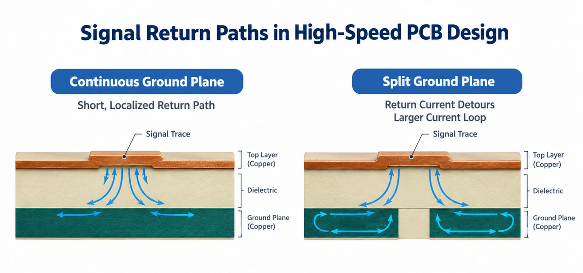
- Return current follows the path of least impedance. At high frequencies, return current flows directly beneath the signal trace on the reference plane. If the reference plane is interrupted, the return current must detour, creating a loop antenna that radiates EMI and distorts the signal.
- Never split reference planes beneath high-speed signals. A signal crossing a plane split experiences impedance discontinuity and increased EMI. Refer to signal integrity literature (e.g., Howard Johnson, High-Speed Digital Design) for detailed analysis.
The figure below contrasts return current behavior over a continuous ground plane versus a split plane where the return path is forced to detour.
- Minimize via stubs. The unused portion of a through-hole via acts as a resonant stub causing insertion loss at high frequencies. Use back-drilling or blind/buried vias to eliminate stubs. JetH PCB supports back-drilling—confirm specific tolerances during DFM review.
- Apply the 3W rule for crosstalk mitigation. Maintain at least 3× trace width as spacing between critical high-speed traces. This empirical rule does not substitute for full crosstalk simulation.
- Manage glass weave effects. FR-4's glass fiber (Dk ~6) and epoxy resin (Dk ~3–4) can cause differential pair skew at multi-gigabit rates. Mitigation includes spread-glass materials or layout rotation relative to the glass weave axis.
Power Distribution Network (PDN) Design
FPGA PDN design is particularly demanding because of high transient currents. Depending on the device, a core supply may draw tens to over a hundred amperes at sub-1V voltages with rapid current step changes. Always refer to the target FPGA's power supply guide for specific requirements.
Key PDN design principles:
- Target impedance: Z_target = ΔV_ripple / ΔI_transient. Achieving low target impedance across the relevant frequency band requires plane capacitance, bulk capacitors, and high-frequency decoupling capacitors working together.
- Plane pair capacitance: Adjacent power and ground planes with thin dielectric form a distributed capacitor providing high-frequency decoupling, complementing discrete decoupling capacitors. Placing PWR and GND planes adjacent with minimal dielectric thickness directly reduces PDN impedance.
- Decoupling capacitor strategy: Use a tiered approach based on the target FPGA's PDN design guide: bulk capacitors near the regulator, mid-frequency capacitors near the FPGA power pins, and high-frequency capacitors as close as physically possible. Specific values should be determined from the FPGA's power integrity analysis, not generic defaults.
- Multiple via connections: Each power pin should connect to the power plane through multiple vias to reduce current density and parasitic inductance.
Material Selection for High-Speed FPGA PCBs
Material choice affects signal loss, impedance stability, and thermal performance. The dielectric loss tangent (Df) is the primary parameter for high-speed signal loss. Actual parameter values vary by product, test frequency, and test method—verify from manufacturer datasheets:
| Material Category | Dk Range | Df Range | General Use Context |
|---|---|---|---|
| Standard FR-4 | 4.0–4.6 | 0.015–0.025 | Low-speed digital, short trace lengths |
| High-Tg FR-4 | 3.8–4.4 | 0.012–0.020 | Industrial digital, moderate trace lengths |
| Mid-loss | 3.4–3.8 | 0.006–0.012 | Higher-speed digital with moderate loss budget |
| Low-loss | 3.0–3.6 | 0.002–0.006 | Long high-speed channels, tight loss budgets |
| Ultra-low-loss | 2.8–3.4 | <0.002 | Very high data rates with stringent loss requirements |
| PTFE-based | 2.1–3.2 | 0.0009–0.003 | RF/microwave, lowest loss applications |
Tg values vary significantly by specific product grade and test method—always verify from the manufacturer's datasheet rather than relying on category-level estimates.
Material selection should be based on the channel loss budget, trace length, dielectric loss, copper foil roughness, and target insertion loss at the operating frequency—not solely on data rate. For specific materials, refer to the manufacturer's datasheet for accurate Dk, Df, and processing parameters. JetH PCB's material capability spans standard FR-4 through ultra-low-loss and PTFE-based systems.
BGA Escape Routing for FPGA Packages
BGA escape routing—routing signals from the solder ball array to accessible routing channels—is often the single most challenging aspect of FPGA PCB layout and frequently determines minimum layer count.
The Four Key Variables
BGA escape routing is governed by four interrelated variables:
| Variable | What It Determines | Impact on Layer Count |
|---|---|---|
| BGA pitch | Spacing between adjacent solder balls; determines available routing channels between pads | Smaller pitch → fewer channels → more layers needed |
| Trace/space | Minimum trace width and spacing your manufacturer can achieve | Finer traces → more channels per gap → fewer layers |
| Via structure | Through-hole, blind, buried, microvia, or via-in-pad | Advanced vias (microvia, VIPPO) access inner layers more efficiently |
| Escape layers | Number of signal layers needed to fan out all BGA pins | Directly determines minimum signal layer count |
A Rough Estimate of BGA Escape Layers
A simplified empirical estimate provides a first-order sanity check for escape layer planning. This is not an industry-standard calculation method—it is a rough estimate based on simplified assumptions that must be validated with actual fanout analysis:
- Depth = number of BGA rows ÷ 2 (from edge to center)
- The outer 2 rows can typically escape on the top layer without vias
- Required inner signal layers ≈ (Depth − 2) ÷ traces per channel
For example, a 16×16 BGA (8 rows deep) with 1 trace per channel suggests (8−2)/1 = 6 inner signal layers. With 2 traces per channel (when channel geometry and via/spacing rules allow two traces between adjacent pads), only 3 inner layers might be needed. The central portion of a typical FPGA BGA is often power and ground pins, which can connect directly to internal planes without routing, potentially reducing the required signal layers.
This estimate does not account for actual solder ball patterns, power/ground pin distribution, via geometry, or routing congestion. Always validate with your actual BGA pinout using PCB layout software's fanout analysis tools. Refer to Altium's BGA fanout design guidelines for additional guidance on evaluating fanout feasibility before finalizing layer count.
BGA Pitch and Routing Strategy
The appropriate routing strategy depends on BGA pitch, but also on pad size, trace/space capability, via geometry, and pin distribution. The following table shows commonly used approaches—not fixed rules. Actual fanout strategy should be determined through layout evaluation:
| BGA Pitch | Common Fanout Approach | Typical Via Type | Possible HDI Approach |
|---|---|---|---|
| 1.27 mm | Dog-bone + through-hole | Mechanical via | Standard multilayer |
| 1.0 mm | Dog-bone + through-hole | Mechanical via | Standard multilayer |
| 0.8 mm | Optimized dog-bone or small via | Blind via often used | Standard or entry HDI |
| 0.65 mm | Small via / HDI / via-in-pad | Laser microvia | HDI may be needed |
| 0.5 mm | Microvia + via-in-pad | Laser microvia / VIPPO | HDI likely needed |
| ≤0.4 mm | Via-in-pad + stacked microvia | VIPPO / ELIC | Advanced HDI likely needed |
The two diagrams below contrast dog-bone fanout with via-in-pad microvias, showing why denser BGA packages demand different escape strategies.
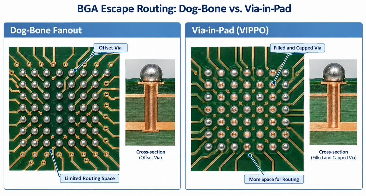
Dog-bone fanout places a via offset from the pad with a short trace connecting them. This is the standard approach for pitches ≥0.8 mm and allows standard through-hole vias.
Via-in-pad (VIPPO) places the via directly within the solder pad, requiring the via to be filled with resin and capped with copper to create a planar solderable surface. VIPPO enables routing from every pad regardless of location, significantly improving routing density for fine-pitch BGA packages and reducing via stub length compared to dog-bone fanout. However, it requires specialized manufacturing capability and increases cost.
HDI Structures for Fine-Pitch FPGA BGA
For fine-pitch FPGA packages, HDI structures may be needed when conventional through-via routing cannot provide sufficient escape channels. Whether HDI is necessary depends on the BGA pitch, pad dimensions, pin distribution, trace/space rules, via geometry, and the available routing layers. Evaluate the actual package and manufacturing constraints before selecting an HDI build-up structure. Common HDI build-up forms include:
- 1+N+1: One microvia layer on each side of a conventional core. The simplest HDI structure.
- 2+N+2: Two microvia layers per side, typically with blind and buried vias in the core. Provides higher density routing.
- 3+N+3: Three microvia layers per side. Used for dense FPGA and mobile processor packages.
- ELIC (Any Layer): Every layer can have microvias. The highest density HDI construction.
Note that IPC-2226 defines HDI types (Type I, II, III) based on microvia layer count and core buried via structure—these do not map one-to-one to the build-up forms above. Refer to IPC-2226 for the official type definitions and design rules.
The cross-section below compares through-hole, blind, buried, stacked, and staggered microvia structures used in HDI fabrication.
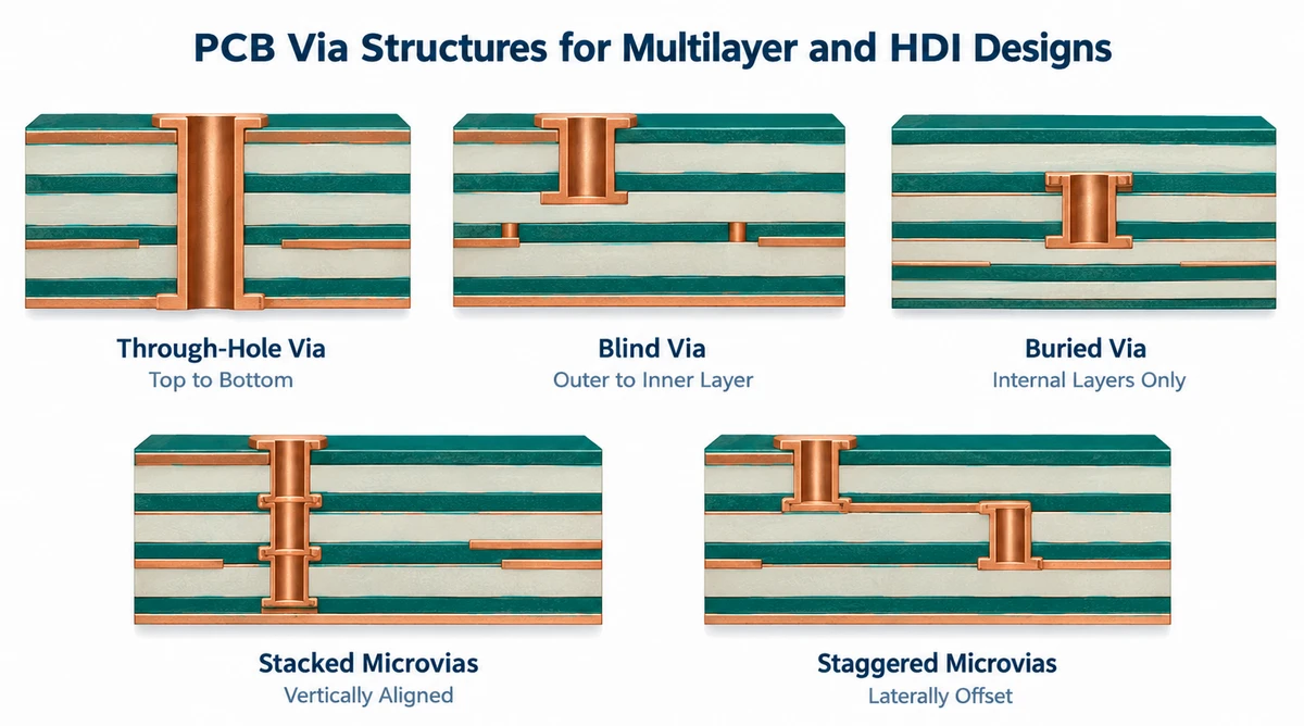
Stacked vs. staggered microvias: Stacked microvias provide the shortest vertical path and highest density but require multiple plating steps. Staggered microvias offer wider manufacturing tolerance and better thermal-mechanical reliability by distributing stress across different layers.
Manufacturing Capability Check
When designing BGA escape routing, verify your manufacturer's capabilities against your design requirements:
| Parameter | What to Check | JetH PCB Capability |
|---|---|---|
| Min laser via diameter | Must be ≤ your design's microvia size | 65 μm production / 50 μm prototype |
| Min annular ring (laser via) | Must accommodate your via + annular ring | 50 μm production / 40 μm prototype |
| Standard trace/space rule (½ oz Cu) | Must be ≤ your routing width/spacing | 62/62 μm production / 50/50 μm prototype |
| VIPPO capability | Required for via-in-pad designs | Supported, 0.15–0.50 mm production / 0.10–0.50 mm prototype |
| Back-drilling | Required for high-speed via stub removal | Supported |
| HDI layer count | Must support your HDI structure | Up to 18 layers production / 32 layers prototype (Anylayer) |
A critical insight: Adding PCB layers does not automatically solve BGA routing problems. If the BGA pitch, minimum trace/space, or via structure cannot accommodate the required routing channels, additional layers alone will not make the design routable. The via structure and routing rules must be evaluated alongside the layer count.
Choosing a Custom PCB Manufacturer for FPGA Boards
Selecting the right custom PCB manufacturer is as critical as the design itself. A manufacturer with insufficient capability will reject your design, produce non-conforming boards, or—worst case—accept the design but fail to meet impedance, registration, or reliability requirements.
Essential Capability Checklist
When evaluating a custom PCB manufacturer for FPGA board production, verify:
- Layer count and HDI: Required layer count in volume, HDI structure support, maximum standard and HDI layer counts
- Minimum features: Trace width/spacing at your copper weight, drill diameter (mechanical and laser), annular ring
- Impedance control: Guaranteed tolerance, TDR test coupons, compatibility with your dielectric materials
- Material range: Low-loss/ultra-low-loss material sourcing, mixed dielectric stackup support
- Special structures: Back-drilling, VIPPO, heavy copper, embedded components (if required)
- Quality system: IPC acceptance class, ISO 9001, 100% electrical testing capability
- Engineering support: DFM review, stackup consultation, impedance calculation support
JetH PCB Manufacturing Capabilities
Based on JetH PCB's manufacturing capability specifications, the following parameters are relevant for FPGA PCB production. For project-specific requirements, confirm current capabilities directly with JetH PCB.
| Capability | Production | Prototype |
|---|---|---|
| Max layer count (non-HDI) | 28 layers | 40 layers |
| Max HDI layer count | 18 layers (Anylayer) | 32 layers (Anylayer) |
| Min laser via diameter | 65 μm (2.6 mil) | 50 μm (2.0 mil) |
| Min annular ring (laser via) | 50 μm (2.0 mil) | 40 μm (1.6 mil) |
| Min trace/space (½ oz Cu, standard design rule) | 62/62 μm (2.5/2.5 mil) | 50/50 μm (2/2 mil) |
| VIPPO via range | 0.15–0.50 mm | 0.10–0.50 mm |
| Back-drilling | Supported | Supported |
| Impedance control (≥50Ω, per production/prototype conditions) | ±8% | ±5% |
| Max copper weight | 6 oz | 14 oz |
JetH PCB's material capability covers standard FR-4, high-Tg, halogen-free, mid/low/ultra-low-loss, PTFE-based, and embedded-capacitor/resistor materials from major suppliers including Rogers, Panasonic, Isola, and leading Chinese laminate manufacturers. Surface finishes include ENIG, ENIPIG, HASL, immersion tin, and hard gold.
Important distinction: These capabilities describe what JetH PCB can manufacture—physical PCB fabrication, not FPGA design, timing closure, or signal integrity simulation. FPGA electrical design, SI/PI analysis, and timing verification remain the responsibility of the design team.
The DFM Review Process
A capable manufacturer should offer a DFM review before committing to production—ideally during the stackup design phase—to check stackup symmetry, minimum feature sizes, via aspect ratios, impedance verification, material availability, and warpage risk. Engaging your manufacturer early can identify constraints before layout is complete, avoiding costly redesign cycles.
From Design to Production: Multilayer PCB Fabrication
Understanding the fabrication process helps designers make decisions that improve manufacturability and yield. Key steps for a typical FPGA PCB:
Fabrication Process Overview
- Engineering review (CAM): The manufacturer's CAM department reviews Gerber files, drill files, and fabrication notes. Stackup is finalized, impedance traces are identified, and panelization is planned.
- Inner layer imaging, etching, and AOI: Copper foil on inner layer cores is patterned using photoresist and etched to form signal traces and plane shapes. Each inner layer is then inspected via automated optical inspection (AOI)—defects found after lamination cannot be corrected.
- Oxidation and lamination: Inner layer surfaces are oxidized to promote adhesion, then cores and prepreg sheets are stacked per the design stackup and pressed under heat and pressure. Stackup symmetry is critical to prevent warpage. Actual lamination conditions depend on the material system, resin chemistry, and manufacturer's process specifications.
- Drilling: Through-holes are mechanically drilled; laser drilling creates microvias for HDI structures. Drill accuracy affects via registration and annular ring integrity.
- Desmear and plating: Drill smear is removed, and holes are metallized via electroless copper plating, followed by electrolytic copper plating to final thickness.
- Outer layer imaging, etching, and soldermask: Outer layer traces are formed using the same photoresist/etch process as inner layers. Liquid photoimageable soldermask (LPI) is then applied, exposed, and developed.
- Surface finish and electrical testing: ENIG, ENIPIG, HASL, or other specified finish is applied to exposed copper pads. Flying probe or bed-of-nails testing verifies continuity and isolation; impedance test coupons may be measured via TDR.
- Singulation: The panel is routed or V-scored to separate individual boards.
IPC Standards Relevant to FPGA PCB Manufacturing
IPC standards provide the acceptance criteria and performance requirements that govern PCB quality. Refer to the IPC Design Standards directory for official documents:
| Standard | Scope | Relevance to FPGA PCB |
|---|---|---|
| IPC-2221 | General PCB design | Base design rules for trace geometry, spacing, via sizing |
| IPC-2226 | HDI PCB design | Design rules for high-density interconnect structures |
| IPC-6012 | Rigid board performance | Qualification and performance requirements for rigid multilayer boards |
When specifying IPC Class 3 (high-reliability) instead of Class 2 (general industrial), expect a cost premium due to tighter tolerances and more stringent inspection criteria. For prototyping, Class 2 is typically sufficient; for production boards in high-reliability applications, Class 3 may be required by customer or regulatory specifications.
Conclusion: Designing Your Custom FPGA PCB
Designing a custom FPGA PCB that balances technical performance, manufacturability, and cost requires a systematic approach:
- Start with the BGA. Evaluate your FPGA package's pin count, pitch, and power/ground pin distribution to estimate the minimum routing layers needed for escape routing.
- Evaluate 6 vs 8 layers against your specific interface requirements, power domain count, and mixed-signal needs. Use the comparison framework in this guide—not a default assumption.
- Design the stackup with proper signal-reference plane pairing, PWR-GND plane pairs for PDN performance, and manufacturing symmetry. Refer to AMD UG583 or Intel AN 315 for device-specific guidance.
- Specify impedance, materials, and tolerances based on your actual interface requirements, not generic defaults. Engage your manufacturer early for DFM review.
- Choose a manufacturer whose capabilities match your design requirements—verify layer count, HDI capability, minimum features, impedance tolerance, and material availability before committing.
For multilayer PCB fabrication of FPGA boards, JetH PCB offers HDI capability up to 18 layers (production) and 32 layers (prototype) with Anylayer construction, laser microvias, VIPPO support, and back-drilling. Their material range covers standard FR-4 through ultra-low-loss and PTFE-based systems, supporting FPGA designs from cost-sensitive industrial applications to high-speed SerDes and mixed-signal RFSoC platforms. Impedance control tolerance of ±8% (production) and ±5% (prototype) is available for impedances ≥50Ω—confirm specific requirements with JetH PCB's engineering team during DFM review.
Request an FPGA PCB Quote
To have your FPGA PCB stackup reviewed for manufacturability or to request a fabrication quote, submit your Gerber files, stackup definition, and fabrication notes to JetH PCB's multilayer PCB manufacturing page. For designs requiring HDI structures for fine-pitch BGA packages, additional capability details are available at JetH PCB's HDI BGA page.
Request a Multilayer PCB Quote | Upload PCB File | Talk to a JetH PCB Engineer