
 中文
A 4-layer PCB stackup defines how the four copper layers in a multilayer board are arranged, what function each layer serves, and how the dielectric materials between them are structured. This arrangement directly determines signal routing space, reference plane availability, power distribution, and controlled impedance performance.
There is no single optimal 4-layer stackup that suits every design. The right configuration depends on your signal types, power requirements, electromagnetic compatibility targets, and manufacturing constraints. This guide compares the standard 4-layer PCB stackup configurations, explains how dielectric thickness and material choices affect the board, and shows how to translate stackup design into controlled impedance and fabrication-ready specifications.
- What Is a 4-Layer PCB Stackup?
- Standard 4-Layer PCB Stackup Configurations
- How to Choose a 4-Layer PCB Stackup Thickness
- How 4-Layer PCB Stackup Design Affects Impedance Control
- Common 4-Layer PCB Stackup Design Mistakes
- What to Provide to a PCB Manufacturer
- Frequently Asked Questions
- Conclusion
- Request a 4-Layer PCB Quote
What Is a 4-Layer PCB Stackup?
A 4-layer PCB consists of four copper layers labeled L1 through L4, separated by dielectric materials. The two outer layers (L1 and L4) are typically used for component placement and signal routing. The two inner layers (L2 and L3) can serve as ground planes, power planes, or additional signal routing layers, depending on the design requirements.
The physical structure typically uses a core-and-prepreg construction:
- Core: A rigid dielectric substrate with copper foil bonded to both sides. The core's dielectric thickness sets the spacing between the two copper layers bonded to it.
- Prepreg (PP): A semi-cured resin-impregnated glass fabric that bonds cores together during lamination. The post-pressing thickness depends on the prepreg style, resin content, and press parameters.
- Copper foil: Applied to outer surfaces and core faces. Common nominal copper foil weights include 0.5 oz/ft² (approximately 17–18 μm), 1 oz/ft² (approximately 35 μm), and 2 oz/ft² (approximately 70 μm). These are nominal thickness equivalents for copper weight, not universal finished-layer thicknesses. On outer layers, the final copper thickness is affected by plating and the fabrication process, so the finished copper specification should be confirmed with the manufacturer.
- Soldermask: Applied to outer surfaces for insulation and protection.
Understanding this construction is essential because the dielectric thicknesses between copper layers — not just the total board thickness — determine trace impedance and signal integrity performance.
Standard 4-Layer PCB Stackup Configurations
Two widely used configurations address different design priorities. The choice between them depends on whether the design requires an independent power plane or prioritizes the quality of the reference planes for signal routing.
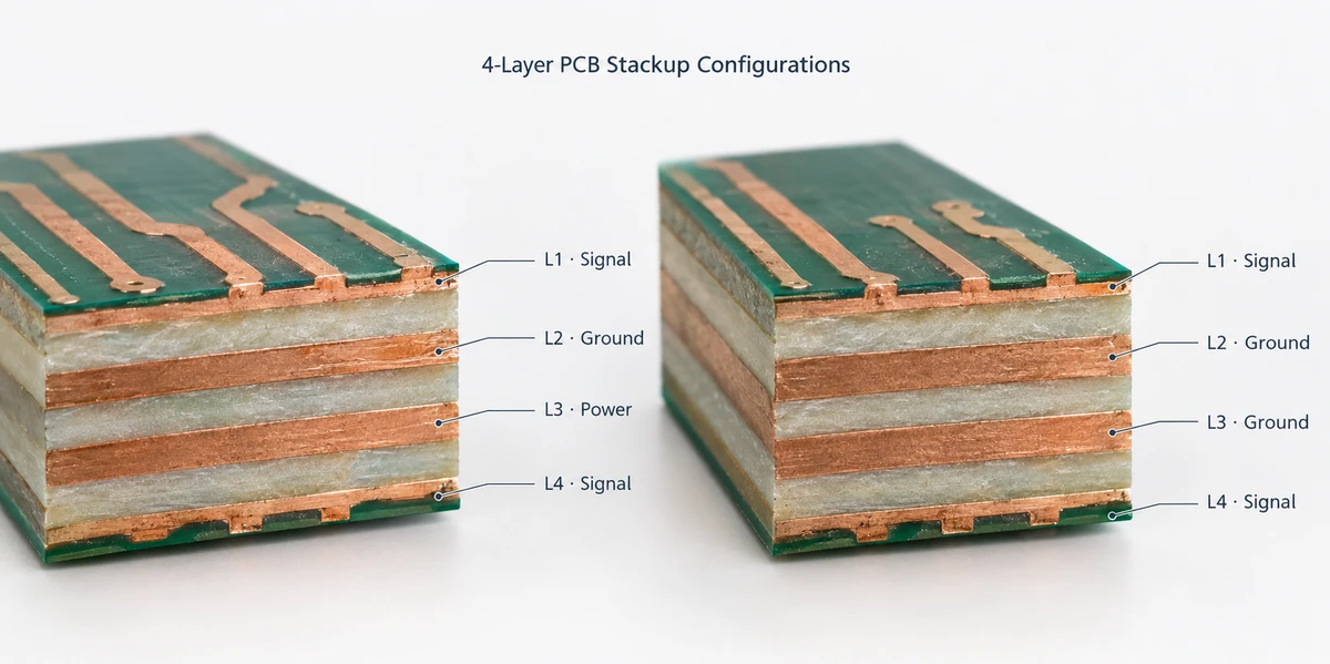
(Comparison of two common 4-layer PCB stackups. The choice depends on power distribution, reference-plane continuity, signal integrity, and manufacturing constraints.)
Signal–Ground–Power–Signal (SIG-GND-PWR-SIG)
This is the classic 4-layer stackup: L1 (signal), L2 (ground), L3 (power), L4 (signal).
Advantages:
- L1 has a continuous ground plane on L2 directly beneath it, providing a low-impedance return path for top-layer signals.
- An independent power plane on L3 simplifies power distribution for designs with multiple voltage rails.
- Both outer layers are available for component placement and signal routing.
Design considerations:
- L4 signals reference the L3 power plane. If the power plane is continuous and well-decoupled, this works well. If the power plane is split between multiple voltages, return paths for L4 high-speed signals may be disrupted.
- This configuration is well-suited for designs where power integrity is a priority and signal speeds on the bottom layer are moderate.
Signal–Ground–Ground–Signal (SIG-GND-GND-SIG)
This configuration places ground planes on both inner layers: L1 (signal), L2 (ground), L3 (ground), L4 (signal).
Advantages:
- Both outer signal layers have a continuous ground plane directly adjacent, providing consistent reference planes and short return paths.
- This arrangement can be advantageous for high-speed digital designs where signal integrity and controlled impedance are the primary concerns.
- When the dielectric construction and copper distribution are also balanced, this symmetric layer arrangement can help reduce board warpage during lamination.
Design considerations:
- There is no dedicated internal power plane. Power must be distributed through traces and copper pours, with appropriate decoupling capacitors placed near the power pins of the relevant components.
- This configuration works best when power distribution is simple (few voltage rails) and signal integrity is the dominant requirement.
Alternative Four-Layer Stackups for Specialized Designs
Other arrangements, such as GND–SIG/PWR–SIG/PWR–GND (outer layers as ground, internal layers for signal and power routing), are used for designs with specific shielding, ESD, or routing requirements. These configurations trade signal layer accessibility for electromagnetic shielding and should be evaluated based on the specific coupling, reference path, and component connection requirements of the design. They are useful for particular applications but are not the default choice for most 4-layer PCB designs.
Key takeaway: No single 4-layer stackup is universally optimal. The configuration should be selected based on signal type, power distribution needs, return path requirements, and manufacturing constraints.
How to Choose a 4-Layer PCB Stackup Thickness
Choosing the thickness of a four-layer PCB involves more than specifying the finished board thickness. Three distinct concepts must be understood:
| Concept | Description |
|---|---|
| Finished board thickness | The total thickness of the completed PCB, including all copper, dielectric, and soldermask layers. |
| Core thickness | The dielectric thickness of the rigid core substrate, which defines the spacing between the two copper layers on each side of the core. |
| Prepreg thickness | The post-lamination thickness of the semi-cured bonding material, which is influenced by prepreg style, resin content, and press parameters. |
Common prepreg styles and their approximate post-pressing thicknesses provide a practical reference for 4-layer stackup planning:
| Prepreg Style | Approximate Post-Press Thickness |
|---|---|
| 1080 | 0.07 – 0.09 mm |
| 2116 | 0.11 – 0.13 mm |
| 7628 | 0.19 – 0.22 mm |
These are approximate pressed-thickness ranges for reference. Actual values depend on the laminate system, resin content, copper coverage, and lamination construction. Confirm the applicable values with the PCB manufacturer before finalizing a controlled-impedance stackup.
The same finished board thickness can correspond to different internal constructions. For example, a 1.6 mm finished 4-layer board can be built with different core and prepreg combinations, each producing different dielectric thicknesses between signal and reference layers — and therefore different trace impedance values.
For a typical four-layer PCB, 1.6 mm is a commonly used finished thickness, but it is not a fixed standard. The actual stackup must be confirmed with the manufacturer based on available materials and the specific prepreg and core combinations they support. Material selection — such as standard FR-4 grades (e.g., S1000-2M from Shengyi) or high-frequency laminates (e.g., Rogers RO3003C) — also affects dielectric constant (Dk) and therefore impedance.
For an overview of the production equipment and processes involved in multilayer lamination, see our PCB manufacturing facilities.
How 4-Layer PCB Stackup Design Affects Impedance Control
Impedance control is where stackup design moves from structure to engineering. The dielectric arrangement in a 4-layer stackup directly determines whether trace impedance targets can be met.
Key Factors That Determine Trace Impedance
| Factor | Effect on Impedance |
|---|---|
| Dielectric thickness | Thicker dielectric between trace and reference plane → higher impedance; thinner → lower impedance. |
| Dielectric constant (Dk) | Higher Dk → lower impedance for the same trace geometry. Different materials (FR-4 vs. high-frequency laminates) have different Dk values. |
| Copper thickness | Thicker copper → slightly lower impedance; also affects etch geometry and achievable trace width tolerance. |
| Trace width | Wider traces → lower impedance; narrower traces → higher impedance. |
| Differential pair spacing | Closer spacing between pair traces → lower differential impedance; the coupling is also influenced by dielectric thickness. |
| Reference plane continuity | Gaps or splits in the reference plane can interrupt return-current paths and introduce impedance discontinuities. |
| Soldermask | The soldermask changes the dielectric environment around outer-layer traces and can affect their impedance. Include it in the impedance calculation when required by the design and fabrication process. |
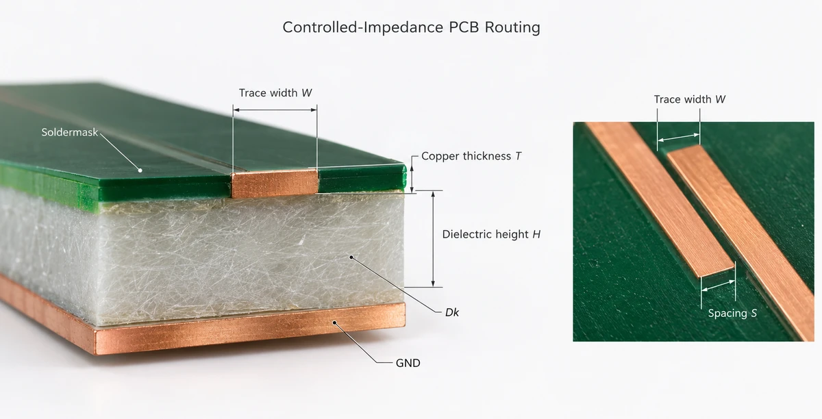
(Controlled impedance depends on trace geometry, dielectric properties, copper thickness, soldermask, and the reference-plane arrangement. The dimensions shown are illustrative, not fabrication specifications.)
Choosing Single-Ended and Differential Impedance Targets
Single-ended impedance is often specified at 50 Ω for high-speed signal traces. Differential impedance targets depend on the interface and the applicable design requirements. Common examples include 90 Ω for USB, 85 Ω for PCIe, and 100 Ω for LVDS. These values are illustrative rather than universal; follow the relevant interface specification and component vendor's layout guidelines.
A 4-layer PCB can support controlled impedance on selected signal layers when the stackup provides a suitable reference plane and the required trace geometry can be achieved for the target impedance.
From Stackup Design to Impedance Verification
The engineering flow for impedance control in a 4-layer PCB follows these steps:
- Define impedance targets — Determine single-ended and/or differential impedance requirements from interface specifications.
- Define the stackup — Select layer arrangement, core thickness, prepreg type, copper weight, and material.
- Calculate trace geometry — Use a field solver or impedance calculator to determine the trace width (and differential spacing) needed for the target impedance given the stackup.
- Manufacturing review — Submit the proposed stackup and impedance requirements to the PCB manufacturer for feasibility review. The manufacturer confirms whether the requested dielectric construction and impedance tolerances are achievable with available materials.
- Verification — After fabrication, impedance can be verified through test coupons or measurement structures included in the panel design.
JetH PCB supports controlled impedance manufacturing with mass-production tolerances of ±4.5 Ω for impedances below 50 Ω and ±8% for impedances at or above 50 Ω. For prototyping and sample builds, tighter tolerances of ±3 Ω and ±5% respectively are available. These tolerances represent specific manufacturing capabilities; the applicable tolerance for a given order depends on the stackup, material, and design complexity, and should be confirmed during the manufacturing review process.
For more on multilayer PCB manufacturing capabilities and impedance-controlled fabrication, visit our multilayer PCB manufacturing page.
Common 4-Layer PCB Stackup Design Mistakes
| Mistake | Why It Happens | Correct Approach |
|---|---|---|
| Reusing trace widths from another design without confirming the stackup | Trace impedance depends on dielectric thickness and Dk, which vary between stackups. | Recalculate or re-simulate trace geometry for the actual stackup of the current design. |
| Routing high-speed signals across a reference-plane split | The split interrupts the return-current path, potentially increasing loop area, impedance discontinuities, and EMI. | Avoid routing high-speed signals across gaps in their reference plane. When a signal changes reference planes, provide an appropriate low-inductance return path using suitably placed stitching vias or decoupling capacitors, depending on the transition. For a detailed discussion of return-current paths and ground splitting, see TI's High-Speed Layout Guidelines (SCAA082). |
| Specifying only board thickness without impedance requirements | Board thickness alone does not define impedance; the internal dielectric arrangement matters. | Provide the full stackup, including core/prepreg thicknesses, copper weight, material, and target impedance values. |
| Finalizing the stackup after routing is complete | Late stackup changes can require trace width adjustments, layer reassignment, and fabrication rework. | Define and review the stackup before routing begins, in coordination with the manufacturer. |
What to Provide to a PCB Manufacturer
To ensure your 4-layer PCB stackup is manufactured correctly with impedance control, provide the following information to your fabrication partner:
- Layer count and proposed stackup — Layer sequence (e.g., SIG-GND-PWR-SIG) with the proposed arrangement.
- Finished board thickness and copper weight — Total board thickness and copper weight for each layer (inner and outer).
- Material requirements — Specific laminate and prepreg materials (e.g., FR-4 standard Tg, high-Tg, or high-frequency laminates), or performance requirements if specific brands are not mandated.
- Target impedance and tolerance — Single-ended and/or differential impedance values with acceptable tolerances.
- Controlled signal layers and reference layers — Which layers carry controlled-impedance signals and which layers serve as their reference planes.
- Trace width and differential spacing — The calculated trace geometries for each impedance target.
- Gerber/ODB++ files and fabrication notes — Complete manufacturing data with stackup diagram and fabrication notes.
- Impedance verification requirements — Whether impedance test coupons are required and which impedance values should be verified.
The manufacturer reviews these requirements against available materials, process capabilities, and design rules to confirm manufacturability. A stackup that works on paper may need adjustment based on the manufacturer's available core and prepreg combinations.
Frequently Asked Questions
What is a typical 4-layer PCB stackup?
A commonly used 4-layer PCB stackup is SIG-GND-PWR-SIG (signal-ground-power-signal), where L2 is a ground plane and L3 is a power plane. Another widely used option is SIG-GND-GND-SIG (signal-ground-ground-signal), which can be advantageous when continuous ground reference planes are a priority. The best choice depends on the specific design requirements.
Is 1.6 mm the standard thickness for a 4-layer PCB?
1.6 mm is a widely used finished thickness for 4-layer PCBs, but it is not a fixed standard. The same 1.6 mm finished thickness can be achieved with different core and prepreg combinations, resulting in different dielectric thicknesses and impedance values. The actual stackup should be confirmed with the manufacturer based on the design's impedance and signal integrity requirements.
Which is better: SIG-GND-PWR-SIG or SIG-GND-GND-SIG?
Neither is universally better. SIG-GND-PWR-SIG provides a dedicated power plane and is suitable for designs with moderate signal speeds and multiple power rails. SIG-GND-GND-SIG provides both signal layers with adjacent ground reference planes, which is advantageous for high-speed signal integrity, but requires power distribution through traces and copper pours. The choice should be based on the design's signal, power, and EMI requirements.
Can a 4-layer PCB support controlled impedance?
Yes. A 4-layer PCB can support controlled impedance on selected signal layers when the stackup provides a suitable reference plane and the required trace geometry can be achieved. The impedance depends on the dielectric construction, material properties, copper thickness, trace geometry, and relevant surface-layer conditions. The proposed stackup and trace dimensions should be reviewed with the manufacturer before fabrication.
Conclusion
Selecting the right 4-layer PCB stackup requires understanding how layer arrangement, dielectric thickness, material properties, and copper weight interact to determine signal integrity and impedance performance. There is no universal best configuration — the optimal stackup depends on your specific signal types, power distribution, and manufacturing constraints.
To move from design to production, provide your PCB manufacturer with the complete stackup specification, including layer sequence, materials, copper weights, target impedance, and verification requirements. This ensures the fabricated board matches your design intent and impedance targets.
Request a 4-Layer PCB Quote
Ready to have your 4-layer PCB stackup reviewed? Submit your layer structure, material requirements, finished thickness, copper weight, and impedance targets to JetH PCB's multilayer PCB manufacturing page for a manufacturing feasibility evaluation. If you are designing an FPGA board and comparing higher layer counts, see our FPGA PCB stackup guide comparing 6-layer and 8-layer designs.
Request a Multilayer PCB Quote | Upload PCB File | Talk to a JetH PCB Engineer