
 中文
JetH PCB has been making high-density interconnect (HDI) printed circuit boards in Shenzhen, China, for 15 years. Over that time, we have overcome the technical challenges of blind and buried via fabrication in second- and third-order HDI printed circuit boards. These HDI PCB stack-ups 2+N+2 and 3+N+3 structures demand advanced HDI blind and buried via fabrication techniques.
Today, we’re taking a closer look at the stack-ups 2+N+2 and 3+N+3 structures of HDI PCBs with blind and buried vias—two technically demanding high-density interconnect constructions.
Published by JetH PCB
HDI PCB Structures at a Glance
- Manufacturer
- JetH PCB, Shenzhen, China
- 2+N+2
- Second-order HDI; two sequential build-up stages
- 3+N+3
- Third-order HDI; three sequential build-up stages
- Via structures
- Blind and buried vias; staggered and stacked microvias
What Does HDI Order Mean in 2+N+2 and 3+N+3 PCB Stack-ups?
The term of “order” refers to the sequential build-up stages, each involving a separate lamination and laser-drilling cycle, rather than the PCB’s total layer count. 2+N+2 (also called Second-order) HDI uses two such stages; 3+N+3 (also called third-order) uses three.
Both the constructions are key to pushing routing density to its limits in today’s high-end precision PCBs.
Explore multilayer PCB manufacturing, custom stack-ups and impedance control.
Second-Order HDI PCB Construction: Staggered and Stacked Microvias
The HDI stack-up structure 2+N+2 requires two separate cycles of lamination, drilling, and plating to complete the blind and buried via structure. Typical configurations fall into two categories:
Staggered Microvias in 2+N+2 HDI PCBs
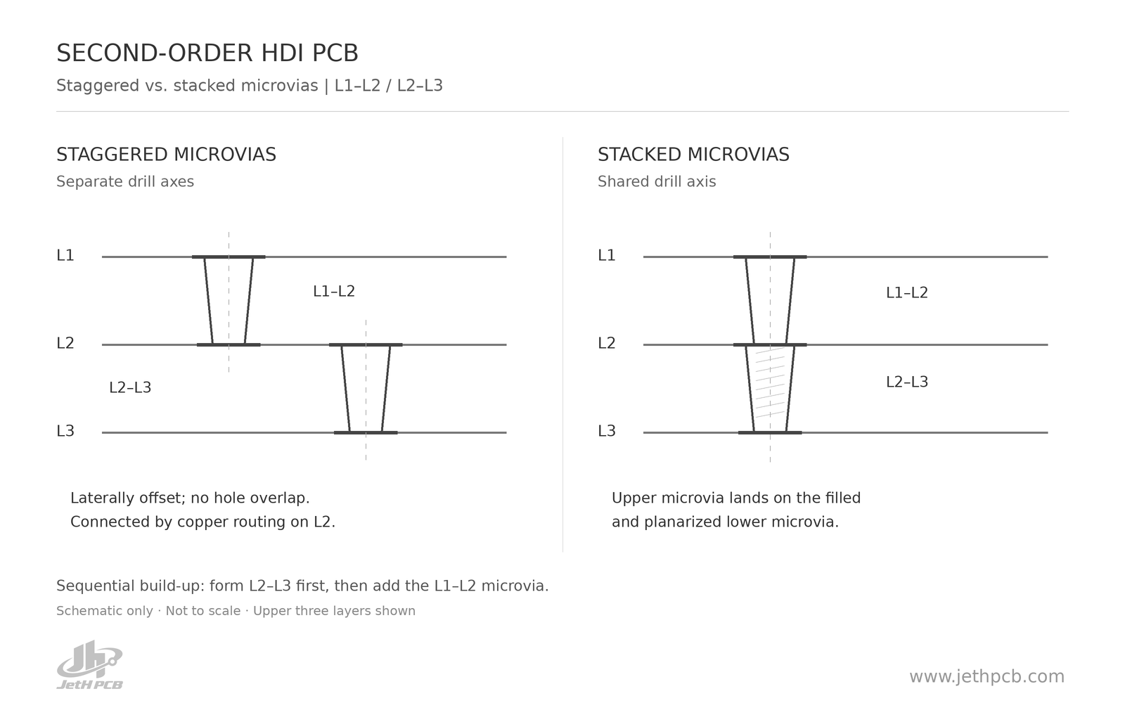
For our 2nd-order HDI, to ensure maximum manufacturability in high-volume production, JetH PCB suggests that it will be a priority to implement a staggered microvia architecture for the L1–L2 and L2–L3 layers. Because the hole centers are physically offset and non-overlapping, this design avoids complex stacked-via constraints, making it our most established 2nd-order HDI process.
As a Chinese PCB manufacturer with more than 15 years of HDI PCBs experience, we feel responsible for explaining the process behind that distinction.
Since staggered vias are drilled and laminated, they don't need to align on the same axis. This gives us much better alignment tolerance, as long as the pad size and clearance requirements are met.
Stacked Microvias: Alignment, Cost and Production Yield
Stacked vias are a different story—they need strict X-ray alignment. You fill and planarize the inner L2–L3 via first, then stack the L1–L2 via right above it. Any misalignment will directly hurt our production yield. JetH PCB keep the yield up.
Here’s the cost and manufacturability trade-off: staggered microvias are 30% cheaper with 95% plus yield. The only area we’ll allow stacked is under the sub-0.4mm BGA to open up routing. So let’s contain the stacked vias strictly to that BGA footprint.
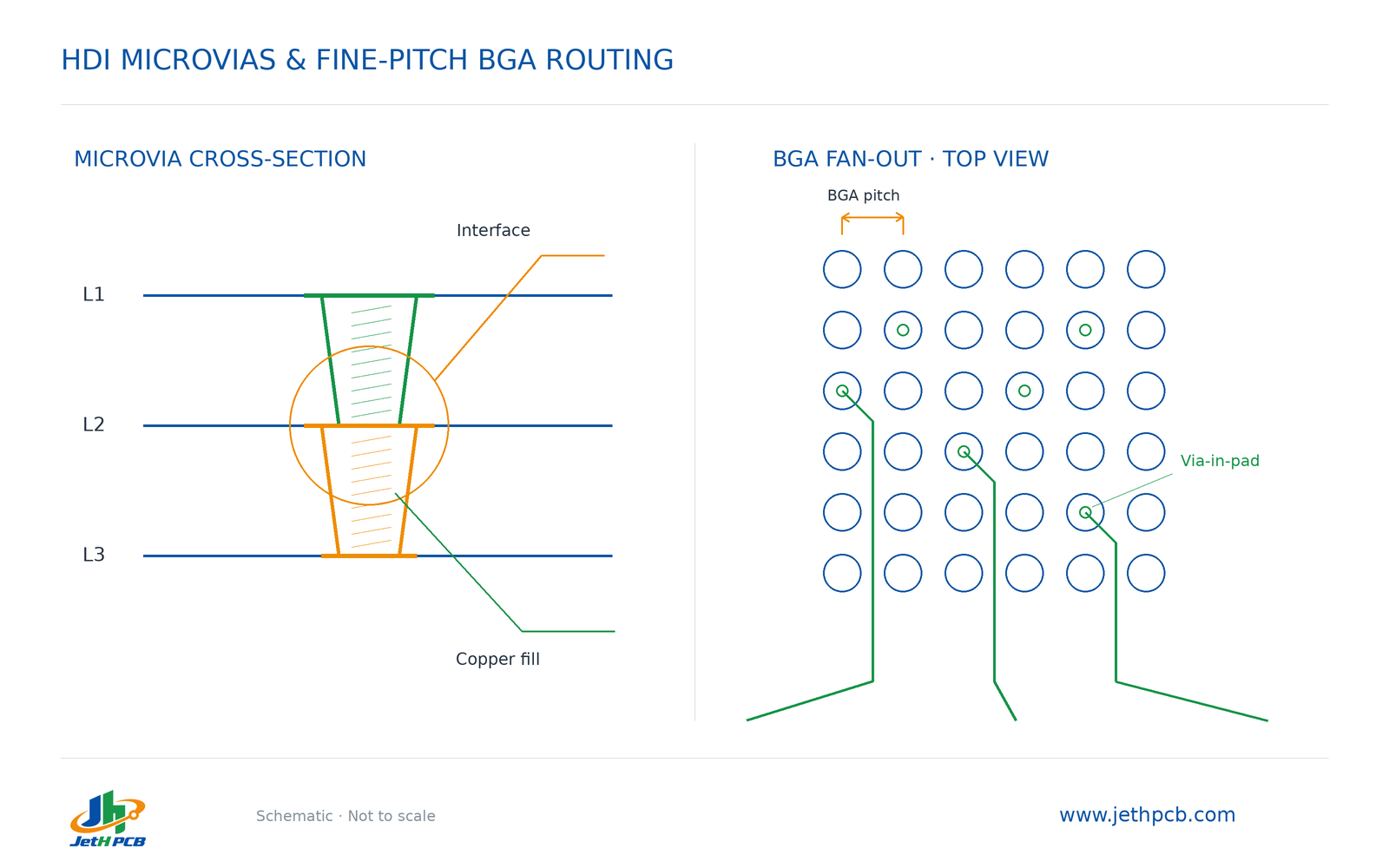
It will be an extreme example if the HDI layout designer is dealing with sub-0.35mm ultra-fine BGA regions, stacked microvias push 2nd-order HDI limits to gain an extra 30% routing density over staggered alternatives. However, they call for strict manufacturing precision: 100% via-to-pad landing, drill offset under 15 μm, and plating dimples below 10 μm. Because yield drops to roughly 80%, an extra 100% X-Ray inspection step is required to catch defects.
Key Process Specs to Watch in JetH PCB:
We cannot cross the rules: layer registration within 25 μm, standard laser drilling at 0.1 mm, plating dimples capped under 12 μm, and an aspect ratio locked strictly at 1:1.2—otherwise, you're just asking for plating voids. We will get 35% more routing space to easily clear 0.4mm BGAs, plus shrunken traces that completely tame stub resonance at 25Gbps.
Q: Where is the structure 2+N+2 HDI PCBs with staggered microvias typically applied?
A: You’ll typically find them in high-performance hardware, such as top-tier GPUs, AI accelerators, server mainboards, and gaming smartphones. If your design is pushing data through blazing-fast interfaces like DDR5 and PCIe 5.0, this architecture ensures your signal integrity stays rock-solid.
Reference cases
Third-Order HDI PCBs: 3+N+3 Build-up and Lamination Shrinkage Control
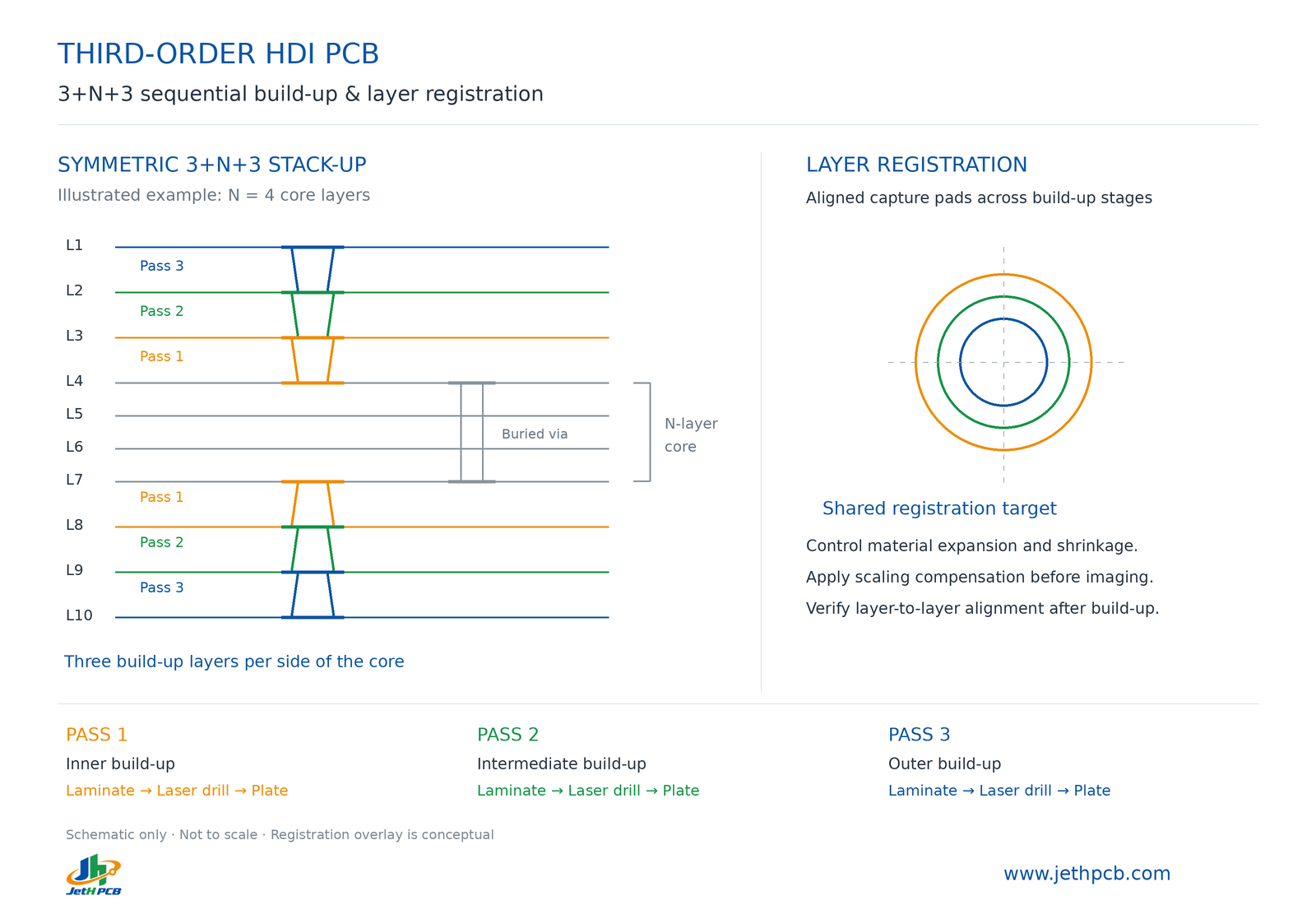
3+N+3, as the absolute peak of mainstream mass production, it takes three separate build-up passes of lamination, laser drilling, and plating. While standard designs can span L1–L4 (or custom-engineered spans like L1 to L5) to use stacked or staggered vias. However, anylayer tech lets you drop microvias between any adjacent pair of layers freely.
This is where top-tier HDI printed circuit boards manufacturer truly stand out. It all comes down to shrinkage control across three lamination cycles- managing material expansion and resin shrinkage through three lamination cycles. Keeping the cumulative offset locked within ±40 μm (and ≤ 15 μm per stage) is a high-wire act that standard 2+N+2 HDI PCB factories simply can’t land.
6-Layer 2+N+2 HDI Example: LDI and Dynamic Sectional Scaling Compensation
Take a 6-layer 2+N+2 stack-up as a classic example: The process sequence kicks off with L3–L4 buried vias in the core. The first build-up pass adds L2–L3 microvias, and the second pass completes the L1–L2 microvias on top. In order to keep every microvia dead center on its target pad across two press cycles, JetH PCB processed HDI by LDI (Laser Direct Imaging) paired with dynamic sectional scaling compensation. That leads 100% via-to-pad alignment and LDI with dynamic sectional scaling.
To handle this HDI stack-up 2+N+, JetH PCB enforces dynamic sectional scaling compensation to hold single-stage alignment within 15μm.
What are the process limits and performance advantages of 3rd-order HDI PCBs?
Process Control Limits for HDI PCB:
Must leverage LDI (Laser Direct Imaging) and plasma descum to reliably hit 0.05 mm microvias. Locks layer-to-layer registration within ±15μm, and applies micron-level pre-compensation for three-cycle lamination distortion—setting a yield barrier far beyond 2-build HDI.
Core Performance:
But the payoff is huge: you unlock 40% more routing real estate, clear tight 0.3 mm BGAs with ease, squeeze the total profile under 0.8 mm, and trim high-frequency signal loss by 20%.
For material and impedance requirements, explore our RF and microwave PCB manufacturing solutions.
Where are HDI PCBs with 3+N+3 structures typically applied?
Any build requiring terabit-level data throughput and minimal footprint:
- Flagship Mobile SoCs: Enables dense fan-out for application processor substrates.
- 5G AAU Transceivers: Protects RF signals from thermal and registration drift.
- Enterprise FPGA Boards: Clears multi-gigabit channels with tight 0.3mm BGA pitch.
- SATCOM Avionics: Squeezes maximum routing density into weight-restricted profiles.
How do 2-build and 3rd-order HDI PCBs compare in core specifications?
| Key Specification / Metric | 2-Build HDI (2+N+2) | 3rd-Order HDI (3+N+3) |
|---|---|---|
| Lamination Cycles | 2 sequential passes | 3 sequential passes |
| Min. Production Via Diameter | 0.10 mm | 0.05 mm |
| Layer-to-Layer Registration Drift | ≤25μm | ≤15μm |
| Routing Density Gain (vs. 1-build) | +35% | +75% |
| Target BGA Pitch | 0.4 mm | ≤0.3 mm fine-pitch |
| Cost Delta (vs. 1-build baseline) | +40% to +60% | +100% to +150% |
DFM Takeaway: Third-Order HDI, Sub-0.3 mm BGAs and Via-in-Pad Routing
DFM Takeaway:
Absolutely, if you're routing sub-0.3 mm BGAs, it remains the mandatory architecture for sub-0.3 mm fine-pitch BGAs due to three physical constraints:
- Routing Density Cap: staggered vias in HDI 2+N+2 stucture can't handle full BGA pin escape at this density.
- Forcing a 2-build approach pushes layer counts from 6 layers up to 10+ layers.
- Via-in-Pad Advantage: 3rd-order stacked vias route directly in-pad, shrinking board size and slashing net system costs.
IPC References for PCB Design, Qualification and Microvia Testing
The following official resources provide general background on PCB design for manufacturability, rigid-board qualification and test methods. They do not validate the JetH PCB manufacturing figures, yield estimates, cost comparisons or performance gains stated in this article. Applicable requirements and acceptance criteria must be agreed for the specific project.
- IPC Design for Manufacturing: Verify Your Design to IPC Standards
An overview of IPC DFM profiles and the design and performance standards used to develop them, including IPC-2221, IPC-2222, IPC-2226 and IPC-6012.
- IPC-6012F: Qualification and Performance Specification for Rigid Printed Boards
Official public table of contents and scope excerpt covering rigid printed boards, including multilayer constructions with blind vias, buried vias and microvias. This PDF is an excerpt, not the complete standard.
- IPC-TM-650 Test Methods Manual
Official test-method directory, including Method 2.6.27 for convection-reflow thermal stress and Method 2.1.1.3 for microsection preparation of microvia structures.