

 中文
A 4-layer PCB is enough when two signal layers carry the routing and each one sits next to an unbroken reference plane. A 6-layer PCB earns its place when routing density, fine-pitch BGA escape, impedance targets, or power plane structure push past what four layers support. The six-layer board costs more to fabricate, so it pays to know which side of that line a design falls on before layout begins.
This guide compares the standard stackups for both layer counts, explains what the two extra layers contribute, lists the cost drivers behind the price gap, and ends with a decision table you can apply to your own board.
Published by JetH PCB
Typical 4-Layer and 6-Layer Stackups
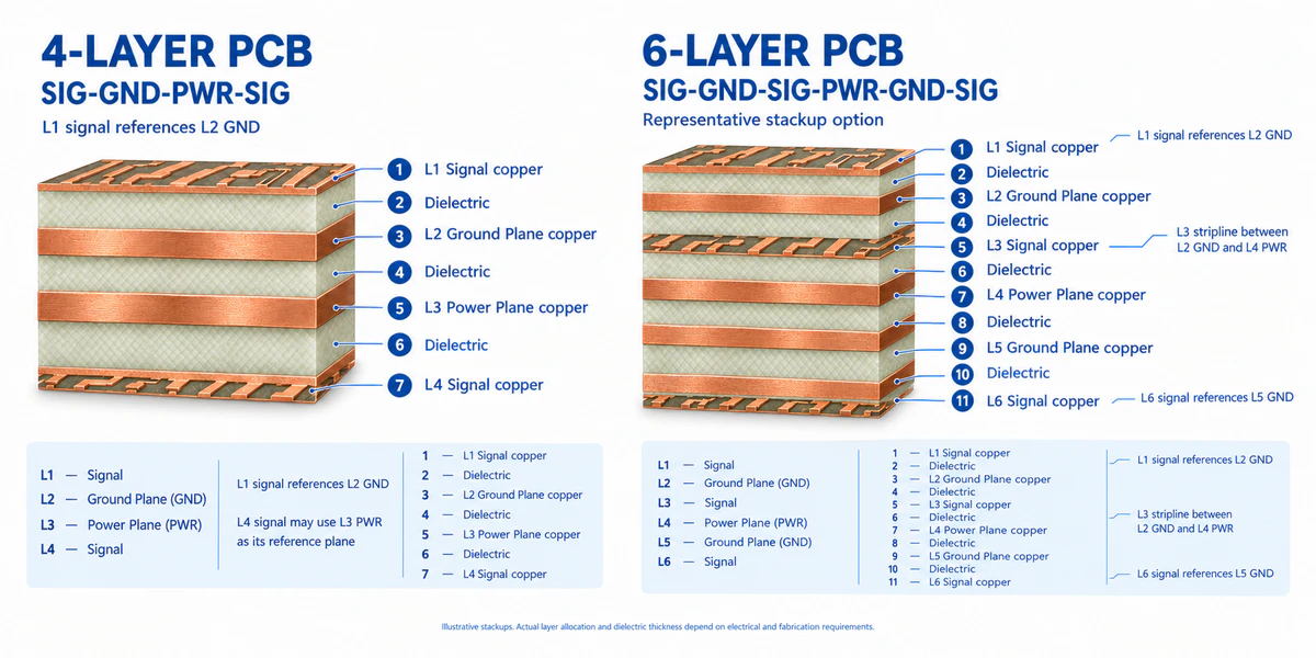
(Four-layer and six-layer builds, side by side.)
The standard 4-layer arrangements
Two common arrangements are:
- SIG-GND-PWR-SIG. L1 and L4 carry components and signals, L2 is a continuous ground plane, and L3 is a power plane. The top layer references solid ground. The bottom layer references the power plane, which works when the region under those traces stays continuous and well decoupled. The risk is localized: where a bottom-layer signal crosses a split in the plane, its return path detours. Multiple voltage rails on one plane are fine as long as the high-speed routes stay clear of the splits.
- SIG-GND-GND-SIG. Both inner layers are ground, so every outer signal layer has a solid reference. This suits low-noise analog and RF sections. Power then travels on traces and copper pours instead of a dedicated plane, with decoupling placed near the loads.
Another possible arrangement is SIG-PWR-GND-SIG. It places a power plane beneath the top signal layer and a ground plane beneath the bottom. It can support controlled-impedance routing when the power plane provides a suitable, continuous reference for the traces above it. Where the plane splits or a signal crosses a discontinuity, the return path has to be evaluated carefully, the same as with any reference plane.
Our 4-layer PCB stackup guide covers these configurations, dielectric thickness selection, and impedance behavior in detail.
Six-layer stackups from documented reference designs
No single standard six-layer stackup exists; the arrangement follows the signal mix and power structure of the design. Two device-vendor reference designs show how the added layers can be allocated:
- Microchip KSZ9692PB layout guidelines (2009). Six layers: L1 signal, L2 ground, L3 signal, L4 signal, L5 power, L6 signal, with 50 Ω single-ended and 100 Ω differential impedance targets. This is a device-specific example with a clear application background, useful for showing a real layer allocation rather than a universal recommendation. (Microchip KSZ9692PB PCB design guideline)
- Microchip SAMA5D2-XULT evaluation board. TOP, GND2, INT3, INT4, VCC5, BOTTOM. The documented build includes specific dielectric thicknesses and a calculated characteristic impedance close to 51 Ω for particular traces, using that board's materials and trace geometry, so the number belongs to that build rather than to six-layer boards in general. In the documented SAMA5D2-XULT design, the relevant region of the VDD plane serves as the reference for bottom-layer DDR3 signals and contains no splits beneath the high-speed routes. A separate Microchip SAMA5D2 layout example shows a power plane divided into multiple voltage domains and cautions against routing high-speed signals across those splits. These examples illustrate why reference-plane continuity must be evaluated against the actual stackup and signal paths. (Microchip AN2717, SAMA5D2 dynamic memory implementation guidelines)
Both examples retain ground and power reference layers while providing four signal layers. This creates more routing options than a typical four-layer arrangement, but whether each signal has a suitable, continuous reference still depends on the plane geometry and the actual route. A common six-layer alternative, SIG-GND-SIG-PWR-GND-SIG, pairs every signal layer with an adjacent plane and routes L3 as stripline between L2 and L4.
The practical takeaway is that six layers can provide more routing capacity and greater flexibility in arranging signal layers and reference planes. The benefit depends on how the additional layers are allocated and whether the resulting stackup addresses the design's actual constraints. More layers alone do not guarantee better performance.
4-Layer vs 6-Layer PCB at a Glance
| Aspect | 4-Layer PCB | 6-Layer PCB |
|---|---|---|
| Signal routing layers | 2 (outer layers) | Up to 4, depending on layer allocation |
| Plane layers | 2, typically GND + PWR | 2, allocated per design (e.g., L2 GND, L5 PWR) |
| Internal stripline routing | Possible, but it costs a plane or surface routing | Available while keeping additional signal layers |
| Controlled impedance | Supported on both signal layers with adjacent planes | More spacing options across signal layers |
| Typical finished thickness | 1.6 mm common | 1.6 mm common |
| Cost | Baseline | Higher, from added material and inner-layer processing |
| Quick-turn fabrication | 48 hours | 48 hours, same window |
| Best for | Designs that route on two layers with unbroken references | Dense routing, fine-pitch BGA escape, many controlled-impedance nets |
Bottom line: Choose 4 layers when the routing fits and every high-speed net has an adjacent unbroken reference plane; move to 6 layers when routing density, escape routing, or plane structure exceed what a suitable four-layer stackup can carry.
What the Extra Layers Buy in Practice
Routing channels. Two additional copper layers can increase available routing channels when they are allocated to signal routing, giving dense designs more flexibility in completing connections. Under a dense connector or a fine-pitch BGA, each row of pins consumes channels on the layers below it, and extra signal layers are often what lets the fanout close at all.
Reference-plane quality. Six layers make it easier to give critical signal layers suitable, dedicated references while preserving enough routing and power-distribution space. On four layers, the bottom layer often ends up referencing a power plane that carries splits. The actual result on either count depends on plane continuity, layer pairing, via transitions, and the routes themselves.
Stripline routing. A signal layer placed between two reference planes can be designed as a stripline. This arrangement helps contain electromagnetic fields within the dielectric and can be useful for critical clocks and other controlled-impedance signals. Some six-layer stackups provide internal stripline routing while retaining additional signal layers and power distribution. Four-layer boards can also use an internal signal layer between reference planes, but this changes the allocation of the remaining layers and may constrain surface routing or power distribution. The advantage of six layers is greater flexibility in balancing routing capacity, reference-plane quality, and power requirements, rather than exclusive access to stripline routing.
Routing Density and BGA Escape Routing
BGA escape routing becomes a limiting factor when signals from inner rows cannot reach their destinations within the available routing channels. Whether additional signal layers or HDI microvias are needed depends on the package pitch, pad geometry, trace and space rules, via dimensions, pin assignment, and fanout strategy. Power and ground balls connect through their own via schemes and unconnected balls need no escape at all, so the constraint is the signals that must cross the pad field, not every ball under the package.
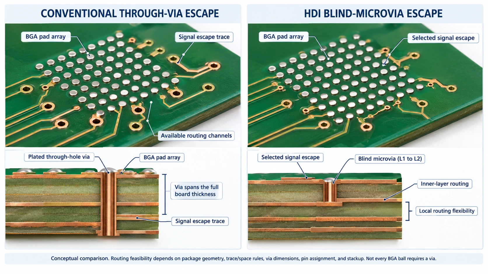
(Through vias versus microvias under the same BGA field.)
At pitches of 0.5 mm and finer, adding plain through-hole layers stops being the only lever, and the decision shifts toward via structure. JetH's engineering guidance for evaluating HDI builds: consider second-order blind and buried via structures around 0.4 mm pitch, third-order for 0.3 mm and finer, with second-order structures generally uneconomical below six total layers. These are evaluation prompts from our fabrication experience, not universal thresholds; the call needs the package and manufacturing conditions in hand. Details on microvia structures are in our HDI PCB for BGA page and the 2+N+2 and 3+N+3 stackup guide.
Impedance Control on 4-Layer and 6-Layer Boards
Controlled impedance depends on the dielectric thickness between trace and reference plane, trace width, copper thickness, and the material's dielectric constant. Both layer counts support it. A four-layer board handles impedance on its two signal layers when each has an adjacent plane and the required trace geometry is achievable. A suitably arranged six-layer stackup can provide internal stripline layers between reference planes and more options for tuning dielectric spacing and trace geometry across multiple controlled-impedance nets.
Manufacturing tolerance is a separate question from geometry. JetH PCB produces controlled-impedance boards with mass-production tolerances of ±4.5 Ω for impedances below 50 Ω and ±8% for impedances at or above 50 Ω, tightened to ±3 Ω and ±5% for prototype and sample builds. These are our stated capability values; the applicable tolerance for a given order depends on the stackup, material, and design complexity, and is confirmed during manufacturing review.
EMI: What Layer Count Changes, and What It Does Not
Return current follows the path of least inductance, which runs directly under its trace on the adjacent plane. A gap in that plane forces the current to detour, the loop area grows, and both radiation and susceptibility rise. On four layers this shows up where bottom-layer routes cross power-plane splits. It shows up on any layer count wherever a high-speed net crosses a plane discontinuity or changes reference planes without a nearby return path. Additional layers help when they enable continuous reference paths, fewer return-path detours, and suitable via transitions; layer count alone does not guarantee lower emissions.
Via stubs are the second mechanism. A through-hole via that spans the full board leaves an unused stub below the last layer it connects, and on thick, high-speed boards those stubs cause reflections. Backdrilling removes the stub. JetH PCB's stated process targets are a residual stub length of 6 ± 4 mil in mass production and 5 ± 3 mil for samples, applied per order during manufacturing review.
Board Thickness and Design Rules
1.6 mm is a common finished thickness for both four- and six-layer boards. Finished thickness does not follow layer count; it follows the dielectric build, and the same 1.6 mm total can be reached with different core and prepreg combinations. For impedance work, what matters is each signal-to-plane spacing, which the fabricator must hit with available materials. A six-layer impedance build specifies those spacings for every controlled layer, which is why the stackup should be agreed with the manufacturer before routing locks.
Cost: What Drives the 4-Layer to 6-Layer Difference
There is no universal cost multiplier for moving from four to six PCB layers. A six-layer board generally costs more because it requires additional material and inner-layer processing, but the actual price difference depends on board size, material selection, copper weight, trace and space requirements, drilling, and order quantity. Design-cost guidance from Altium also identifies layer count, materials, lamination, drilling, and manufacturing complexity as important cost drivers. The most reliable way to establish the difference is to compare quotes based on the same board specifications and fabrication requirements.
What moves the number:
| Cost driver | Notes |
|---|---|
| Layer count | Two additional copper layers mean more laminate, foil, and inner-layer process steps per board |
| Board area | Price scales with the panel area each board consumes |
| Copper weight | Heavier copper tightens etching and plating requirements |
| Via count and type | Blind and buried vias add lamination and drilling cycles |
| Controlled impedance | Cost may come from impedance design verification, test coupons, and additional process control; the adder varies by order |
| Finished thickness and surface finish | Special thickness requirements, premium finishes, and tighter tolerances can affect the quote |
| Material system | High-frequency laminates cost well above standard FR-4 |
Blind and buried vias, microvias, and the extra lamination cycles they require can change a quote materially when a design moves down the HDI path; the structures and their trade-offs are covered in our HDI stackup guide.
To compare quotes fairly, provide each fabricator with the same board specifications and fabrication data. Use IPC-2581 or ODB++ where supported, or provide the required Gerber files, NC drill data, fabrication drawing, stackup, material specifications, and impedance requirements. Confirm each fabricator's preferred file format before submission. Quotes built from different inputs are not comparable.
For standard builds that meet quick-turn and production requirements, four- and six-layer boards share the same turnaround windows at JetH PCB: 48-hour quick-turn fabrication, with typical prototype delivery in 5 days and volume delivery in 8. Quoted lead times exclude engineering review time, normally one day, and are confirmed after file review. Special materials, HDI via structures, controlled-impedance requirements, or additional testing can extend them.
When Six Layers Are Not the End of the Line
FPGA and SoC designs with wide DDR interfaces, many voltage domains, or dense SerDes banks often move to eight layers or more. The trade-offs repeat at each step: more routing and planes against more cost and thickness. Our custom FPGA PCB design guide walks through the 6-layer vs 8-layer decision for those boards. JetH PCB manufactures 2 to 40 layers, with HDI constructions from 1+N+1 to 3+N+3, so the layer count can follow the design instead of the other way around.
How to Choose: Decision Table
| Design condition | Recommended starting point |
|---|---|
| Two signal layers route the design with margin; moderate edge rates; few power rails | 4 layers, SIG-GND-PWR-SIG |
| Low-noise analog or RF sections; simple power distribution | 4 layers, SIG-GND-GND-SIG as a candidate, confirmed against the actual frequency, material, and reference structure |
| Controlled impedance on a handful of nets; routing fits on two layers | 4 layers |
| Dense routing or fine-pitch BGA that two signal layers cannot escape | 6 layers; evaluate HDI microvias as pitch shrinks toward 0.4 mm and finer |
| Many high-speed nets needing stripline and unbroken references on every signal layer | 6 layers |
| Wide DDR buses, many voltage domains, or high-pin-count FPGA/SoC designs | Evaluate 6-layer vs. 8-layer or higher stackups against the actual routing and power-distribution requirements |
Frequently Asked Questions
Is a 6-layer PCB always better than a 4-layer PCB?
No. A six-layer board helps when the added layers buy reference planes, stripline routing, or escape channels. If a four-layer arrangement already gives every high-speed net an unbroken adjacent plane and the routing fits, the extra layers add cost without adding performance.
How much more does a 6-layer PCB cost than a 4-layer PCB?
There is no standard multiplier. A six-layer board generally costs more due to added material and inner-layer processing, but the actual gap depends on area, copper, vias, impedance requirements, thickness, finish, and materials. Quote the same design data to each fabricator to get comparable numbers.
What is an example of a 6-layer PCB stackup?
One documented example is the Microchip KSZ9692PB reference layout: L1 signal, L2 ground, L3 signal, L4 signal, L5 power, L6 signal, with 50 Ω single-ended and 100 Ω differential impedance targets. Another common arrangement, SIG-GND-SIG-PWR-GND-SIG, pairs every signal layer with an adjacent plane. Either way, the final stackup should be confirmed with the fabricator against the actual design.
Can a 4-layer PCB support controlled impedance?
Yes, when each controlled signal layer has a suitable adjacent reference plane and the trace geometry fits the dielectric build. Tolerances at JetH PCB run ±4.5 Ω below 50 Ω and ±8% at or above 50 Ω in mass production, tighter for samples.
Does moving to 6 layers automatically reduce EMI?
No. The reduction comes from how the layers are used: unbroken reference planes under every high-speed net, short return paths, and managed via stubs. A six-layer stackup with poor plane pairing can radiate more than a clean four-layer design.
At what BGA pitch should I stop adding plain layers?
There is no fixed pitch threshold. At 0.5 mm pitch and finer, evaluate HDI microvias alongside layer count. JetH's engineering guidance: second-order blind and buried vias for around 0.4 mm pitch, third-order for 0.3 mm and finer, with second-order structures generally uneconomical below six total layers.
Conclusion
The choice comes down to what the two extra layers would be spent on. When routing fits and every high-speed net already has an unbroken reference plane, four layers are the economical choice, and the standard SIG-GND-PWR-SIG or SIG-GND-GND-SIG builds cover most of those designs. When routing density, escape routing, reference-plane arrangements, or power-distribution requirements exceed what a suitable four-layer stackup can accommodate, a six-layer design may provide the additional routing capacity and design flexibility needed. The actual improvement depends on the layer arrangement, return paths, and routing implementation.
Either way, agree on the stackup with the manufacturer before routing: layer sequence, dielectric thicknesses, copper weights, materials, impedance targets, and tolerances. That review confirms the build is manufacturable at the quoted tolerance before the layout locks.